SDC File in the Logic Synthesis Flow of VLSI Design
SDC (Synopsys Design Constraints) File in the Logic Synthesis Flow of VLSI Design
What is SDC & SDC Introduction?
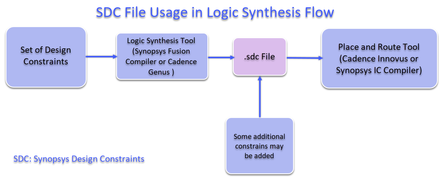
SDC or the Synopsys Design Constraints (SDC) is a common format for constraining the design which is supported by almost all Synthesis including Cadence Synthesis tool Genus and Siemens Synthesis Catapult, and other tools/steps such as PnR. Generally, timing, power and area constraints of design are provided through the SDC file and this file has extension .sdc. SDC file syntax is based on TCL format and all commands of sdc file follow the TCL syntax.

SDC file contains the following information:
- SDC version (optional)
- SDC units (optional)
- Design Constraints
- Design Objects
- Comments (optional)
The information specified in design constraints is operating conditions, wire load models, system interface, design rule constraints, timing constraints, timing exceptions, area constraints, multi-voltage & power optimization constraints and logic assignments.
Design constraints will have all the object access commands. Objects can be design, clock, port, pin, cell, net, library, etc.
We will understand the design constraints with reference to the following figure. We will not look at the syntax of SDC commands. The aim of this blog is to understand how SDC file is written for a design.
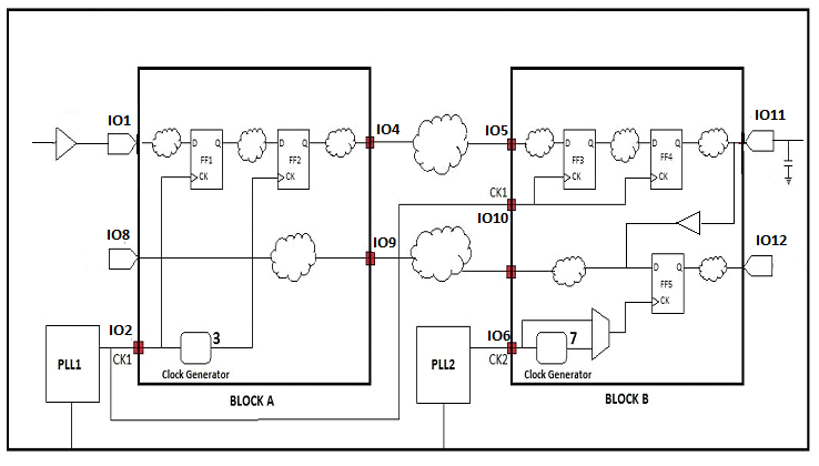
There are two blocks in the design named block A and block B. Two PLLs serve two different clocks to the design. Design constraints will be defined at the I/O pins.
I/O Pins 2, 6, 10 – Clocks are the most important part of a design. As there are two PLLs in the above design, it is clear that there are two different clocks in the design. These clocks must be defined in the timing constraints. At pin IO2 of block A and pin IO6 of block B, the clocks are entering the blocks. Hence are defined using create_clock command at respective pins. This command specifies the period, duty cycle, rise and fall edges of a clock. You can also give name to the clock. Clock CK1 is also going to the clock pins of flops in block 2. So, we have to define clock CK1 at IO10 of block 2 also.
Example:
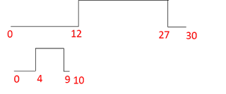
create_clock -period 10 -waveform {0 6} -name my_clk1 [get_ports IO2]
I/O Pin 1 – Input port is applied with the command set_driving_cell. Doing this causes the port to have a cell delay that is load-dependent value of external cell which is driving that port. In the design shown in the figure, buffer is an external cell which is driving the input port of block A. Doing this helps us to have accurate external delay which is required for timing calculations.
Example:
set_driving_cell -lib_cell BUF [get_ports IO1]
Clock generators 3, 7 – There can be a number of clock generator circuits in the given design. Frequency of these generated clocks is different than the master clock. Clock generators can be used for multiplying, dividing or just inverting the master clock to derive a new generated clock. As frequency is changing, we have to define them as new generated clocks at the output of clock generator circuit. create_generated_clock command is used for this purpose. While defining generated clocks, we must specify the master clock.
Example:
create_generated_clock -divide_by 2 -source [get_ports IO2] -name clk_div [get_registers FF2]
I/O Pin 4 – To do constraint checking at the output port, set_output_delay command is used. This command calculates the delay between output port and the next sequential cell (which captures data from this output port.) But when we think about block level design, we will not be knowing that where the output port is connected. Still we should calculate the output delay. To favor this, virtual clock is defined. This virtual clock is same as the normal clock but it does not have any real existence.
Example:
set_output_delay 1.7 -clock my_clk1 [all_outputs]
I/O Pin 5 – Similar to output delay, input delay is calculated. set_input_delay command is used to calculate the timing requirements at the input port. It will calculate timing of the external path to the input port.
I/O Pin 11 – set_load command is used to describe an external load capacitance connected to the top level port. This command considers pin as well as wire capacitance. This command helps us to time the design accurately.
Example:
set_load 20 [get_ports IO11]
As there are two different clocks (i.e. asynchronous clocks) in the design, any path which starts from CK1 and goes to CK2 should not be considered for timing analysis. Best way to achieve this is setting these clock as asynchronous. set_clock_group command specifies whether clock groups are synchronous, asynchronous or exclusive.
In this example, CK1 and CK2 are set as asynchronous clocks. In block 2, the output of mux is going to FF5. Input to the mux are CK2 and a generated clock with CK2 as a master clock. But at a particular instance of time, only one clock will go to the output of a mux. Hence, these two clocks are set as mutually exclusive clocks.
Timing Exceptions:
1. Falsepath:
Some paths in the design need not to be considered for the timing analysis. There can be multiple reasons to set a path as a falsepath. One of the reasons is shown in the above design. CK1 and CK2 are asynchronous clocks, so we set any path from CK1 to CK2 as a falsepath. set_false_path command is used for this purpose. Path from FF4 to FF5 is a false path because both the flops are driven by different clocks.
Example:
set_false_path -from [get_clocks my_clk1] -to [get_clocks my_clk2]
2. Max & Min path:
I/O Pins 8, 9 – The path groups are of four types: input-to-reg, reg-to-output, reg-to-reg and input-to-output. The path from input pin IO8 to output pin IO9 of block A is input-to-output. In such cases, we have to constrain these paths to maximum delay or minimum delay. set_max_delay and set_min_delay commands are used to define these delays.
Example:
set_max_delay 0.15 -from IO8 -to IO9
3. Multi-cycle path:
Data takes one clock cycle to propagate from launch flop to capture flop. But it can also take more than one clock cycle. We should set such paths to multi-cycle path using set_multicycle_path command. Multi-cycle path is always a multiple of the clock cycle.
Constraints & Syntax in the SDC file
SDC file syntax is based on TCL format and all commands of sdc file follow the TCL syntax. Here are the syntaxes and list of constraints with some examples:
In sdc file ‘#’ is used to comment a line and ” is used to break the line. SDC file can be generated by the synthesis tool and the same can be used for PnR.
Constraints in the SDC file
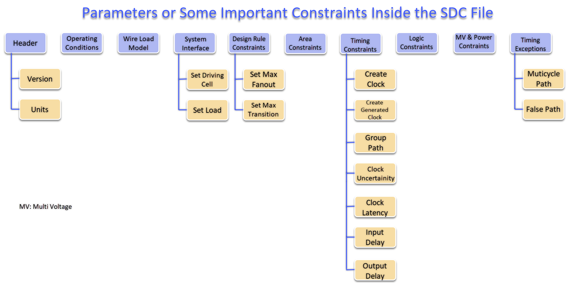
Inside the SDC file, some important constraints are as follows:
1. SDC Version:
This statement specifies the version of the SDC file. it could be 2.1, 2.0, 1.9 or more older.
Version 2.1 has introduced in December 2017.
2. Units:
Units of various quantities like time, resistance, capacitance, voltage, current, and power can be specified using set_unit command.
Multiples units can be set using a single set_unit command.
Example:
A. Operating Conditions
The analysis type can be bc_wc or on_chip_variation. In case of bc_wc (best case/worst case) analysis type, the tool used maximum operating condition for setup checks and minimum operating conditions for hold checks. In case of on_chip_variation mode, maximum operating conditions for all maximum path delays (data paths) and minimum operating conditions for minimum path delays (clock paths).
In any analysis mode, -min and -max option can be used to specify minimum operating condition and maximum operating condition respectively. If the operating conditions are listed in different libraries, they can listed using -min_library and max_library option. If operating conditions are listed in the same library, it can be listed using -library option. The -object_list allows operating conditions to be applied for specified cells or ports.
To view libraries and operating conditions being used in the current design use report_design command. To view all operating conditions present in a particular library, we can use either report_lib -operating_conditions <library_name> or report_operating_conditions -library <library_name>.
create_operating_conditions -name <operating_condition_name> -library <existing_library_name> -process <process_value> -voltage <voltage_value> -temperature <temperature_value> -tree_type <tree_type_name>
create_operating_conditions -name WCCOM -library tech.db -process 1.2 -voltage 2.8 -temperature 30 -tree_type balanced_tree
To remove operating conditions that has been set, we can use remove_operating_conditions.
B. Wire Load Models (WLM)
How do you estimate the parasitics (RC) of a net before placement and routing?
Prior to the Routing stage, net parasitics and delays cannot be accurately determined we know only the fanout of net and the size of the block.
Before going for floorplanning or layout, wire load models (WLM) can be used to calculate interconnect wiring delays (capacitance (C), resistance (R)), and the area overhead (A) due to interconnect.
The wire load model is also used to estimate the length of a net-based upon the number of its fanouts.
The wire load model depends upon the area of the block, and designs with different areas may choose different wire load models.
The wire load model also maps the estimated length of the net into the resistance, capacitance, and the corresponding area overhead due to routing. The average wire length within a block increases as the block size is increased.
Generally, a number of wire-load models are present in the Synopsys technology library, each representing a particular size block of the logic. These models define the capacitance, resistance, and area factor of the net.
Typically a wire load model selection is based upon the chip area of the block. However these WLM models can be modified or changed according to the user’s requirement by the designers.
Figure shows different areas (chip or block size), having different wire load models would typically be used in determining the parasitics (RC), so from the figure, it is clear that the smaller sized block has a smaller capacitance.
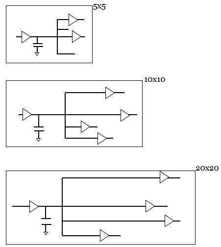
Example of a wire load model
The wire load model specifies slope and fanout_length for the logic under consideration along with Resistance, capacitance, and area overhead. The fanout_length attribute specifies the value of the wire length that is associated with the number of fanouts.
If any fan out number is not explicitly listed in the table, the interconnect length is obtained by using linear extrapolation and interpolation with the specified given slope.
wire_load (“wlm_conservative”) {
resistance: 6.0; # resistance per unit length of the interconnect
capacitance: 1.2; # capacitance per unit length of the interconnect
area: 0.07; # area overhead per unit length of the interconnect.
slope: 0.5; #extrapolation slope used for data points that are not specified in the fan-out length table.
fanout_length (1, 2.6);
fanout_length (2, 3.1);
fanout_length (3, 3.6);
fanout_length (4, 4.1);
fanout_length (6, 5.1);
fanout_length (7, 5.6);
}
fanout_length (2, 2.9) means that for output pin with fanout equal 2, the wire length will be 2.9. Then you need to multiply this wire length with capacitance and resistance to calculate RC values for all wires.
These wire load models are based on statistical info (average wire length among different designs) and doesn’t requires cell placement info (so it is easy, faster method, but not very accurate) i.e. just a rough estimate of the load that can be caused by wires. Wire load model information will be in the liberty files (what we call .libs) provided by the foundry.
Some companies create Custom WLM. – Just to have more accurate WLM for their own designs. They did place (and route) of their design, collect info of all wires (fanout and length for each net), and generate average length per fanout. For example, Synopsys Jupiter has such capability.
Example1: for fan out of 8
Fanout 8 is not present in the table then we used linear extrapolation to calculate the length of interconnect, Resistance, capacitance, and area overhead.
For extrapolation
Length = Length of Last fanout number given in the table + (The fanout number we want – Last fanout number in WLM) * Slope
Capacitance = New calculated Length * Capacitance coefficient given in the table
Resistance = New calculated Length * Resistance coefficient given in the table
Area overhead due to interconnect = New calculated Length * Area coefficient given in the table
So, Length = 5.6 + (8 – 7) * 0.5 = 6.1 units
Capacitance = 6.1 * 1.2 = 7.32 units
Resistance = 6.1 * 6 = 36.6 units
Area overhead due to interconnect = 6.1 * 0.07 = 0.427 units
Example2: for fan out of 12
Length = 5.6 + (12 – 7) * 0.5 = 8.1 units
Capacitance = 8.1 * 1.2 = 9.72 units
Resistance = 8.1 * 6 = 48.6 units
Area overhead due to interconnect = 8.1 * 0.07 = 0.567 units
Example3: for fan out of 5
Since it is between fanout numbers 4 and 6 so we calculate the length using linear interpolation and linear interpolation between the two nearest pairs is used to estimate any points that are not in the lookup table.
For interpolation:
Length = Average of fanout lengths = (Net length at fanout 4 + Net length at fanout 6)/2
Capacitance = New calculated Length * Capacitance coefficient given in the table
Resistance = New calculated Length * Resistance coefficient given in the table
Area overhead due to interconnect = New calculated Length * Area coefficient given in the table
Length = (4.1 +5.1)/2 = 4.6 units
Capacitance = 4.6 * 1.2 = 5.52 units
Resistance = 4.6 * 6 = 27.6units
Area overhead due to interconnect = 4.6 * 0.07 = 0.322 units
The units for the length, resistance, capacitance, and area are as specified in the library.
Wire load Models Types:
Till now we saw that for a particular net we can estimate the RC values as per the WLM. If a net crosses a hierarchical boundary, then different wire load models can be applied to different parts of the net and these wire load modes are of three types:
- Top
- Enclosed
- Segmented
Top:
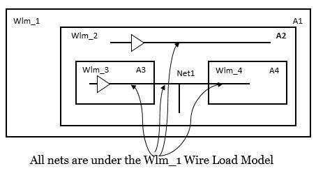
In this mode, all the nets within the hierarchy use the wire load model of the top-level, and if any wire load models specified in lower-level blocks (sub-blocks) then we ignored that WLM model. Only the top-level wire load model takes precedence over all the WLM modes.
From the figure, the wlm_1 wire load model specified in block A1 is used over all the other wire load models specified in blocks A2, A3, and A4.
Enclosed:
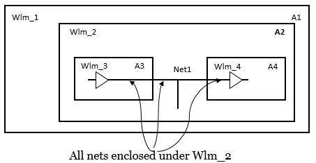
In this WLM mode, the wire load model of the block that fully encompasses the net is used for the entire net.
From the figure, the net Net1 is included in block A2 and thus the wire load model of block A2, wlm_2 is used for this net.
Other net that is fully contained in block A3 use the wlm_3 wire load model, and net that is fully contained within block A4 use the wlm_4 wire load model.
Segmented:
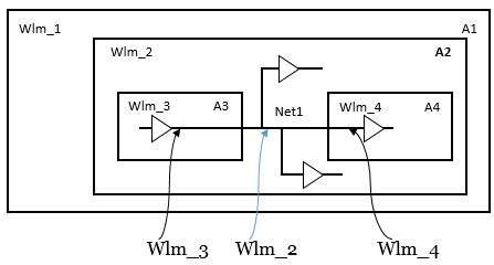
In this WLM mode each segment of the net gets its wire load model from the block that encompasses the net segment. Each portion of the net uses the appropriate wire load model within that block.
Figure illustrates an example of a net Net1 that has segments in three blocks. The interconnect within block, A3 uses the wire load model wlm_3, the segment of the net within block A4 uses the wire load model wlm_4, and the segment within block A2 uses the wire load model wlm_2.
Depending upon the wire_load_mode attribute, the net assumes different wire_load_model based on its span across the chip.The “top” setting causes the wire load model and cell area for the top level to be used. If wire load models are set on sub-designs, it has no effect. This setting model nets as if the design has no hierarchy, it is highly pessimistic.
The “segmented” setting causes the sum of all cell areas of the design containing the net to be used. Nets crossing hierarchy are divided into segments. Each net segment is estimated from the wire load model of the design enclosing the net. If the design enclosing the net has no wire load model set, the design hierarchy is traversed upwards until a wire load model is found.If lower blocks in the design are to be specified a wire load model, then top design must be set to segmented or enclosed mode.
Estimation of wire lengths of pin-to-pin connections are done based on fanout count, and then those estimates are used to calculate net capacitance, net resistance and net area estimates. Fanout is the total number of pins on the net, excluding the driver pin.
Consider a sample library view of only one of its wire load model
wire_load(WL_RCA) {
resistance : 50.0;
capacitance : 2.0;
area : 0.5;
slope : 1.5;
fanout_length(1, 11.5) ;
fanout_length(2, 24.4) ;
fanout_length(3, 38.9) ;
fanout_length(4, 62.7) ;
fanout_length(5, 91.8) ;
fanout_length(10, 156.2) ;
fanout_length(16, 317.8) ;
}
The capacitance, resistance and area values listed corresponds to values per unit length. The value of slope listed is used to extrapolate values outside the range of fanout listed and interpolate values inside the range of fanout listed.
Consider, on a net with 4 fanout pins and 2 fanin pins, the fanout value is
(4+2)-1=5
net_capacitance = 91.8*2.0 = 183.6
net_resistance = 91.8*50 = 4590
net_area = 91.8*0.5 = 45.9While synthesis, this estimated values are used for different optimization possibilities.The set_wire_load_model command can be used to define a wire load model for designs, hierarchical cells and ports. The syntax is:
-name <model_name>
[-library <library_name>]
[-min] [-max]
[object_list]To remove wire_load_model attribute use the remove_wire_load_model command.
wire_load_from_area(0,16000,wm_1);
wire_load_from_area(16000,32000,wm_2);
wire_load_from_area(32000,96000,wm_3);
wire_load_from_area(96000,160000,wm_4);
wire_load_from_area(160000,320000,wm_5);
To remove the wire_load_selection_group attribute, use remove_wire_load_selection_group command.
C. System Interface
Let’s discuss some important System Interface constraints in this section.
3. Set driving cells:
specifies the drive characteristics of input or inout ports that are driven by the cells in the technology library. These commands associate a library pin with input ports so that delay calculation can be accurately modelled.
Syntax:
set_driving_load [-lib_cell lib_cell_name] [-library lib_name] [-rise] [-fall] [-min] [-max] [-pin pin_name] [-from_pin from_pin_name] [-dont_scale] [-no_design_rule] [-input_transition_rise rtrans] [-input_transition_fall ftrans] [-multiply_by_facrtor] [-clock clock_name] [-clock_fall] port_list
4. Set load:
This command sets the load attributes on the specified ports and the nets in the current design. The unit of load value will be the unit of capacitance specified in the unit defined in this file.
D. Design Rule Constraints
In this part basically maximum fanout, maximum and minimum capacitance, and maximum transition time are set
5. Set maximum fanout:
Maximum fanout load is set to a specific input port and/or design
Syntax:
set_max_fanout fanout_value object_list
set_max_fanout 5 [get_ports {port[10]}]
6. Set maximum transition:
Maximum transition time is set by this command which is a design rule and set to clock port or design is set to a specific input port and/or design.
Syntax:
set_max_transition transition_value [-data_path] [-clock_path] object_list
Example:
set_max_transition 2.5 [get_ports IN]
E. Timing Constraints
In this part basically, we set clocks definition, clock group, clock latency, clock uncertainty, clock transition, input delay, output delay, timing derates etc.
7. Create clock:
Syntax:
create_clock [-name clock_name] [clock_sources] [-period value] [-waveform edge_list] [-add] [-comment]
The create_clock command creates a clock object in the current design. This command defines the specified source_objects as a clock source.
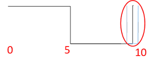
create_clock -name “PH12” -period 10 -waveform {0.0 5.0}
8. Create generated clock:
Syntax:
create_generated_clock [-name clock_name] [-add] source_objects -source master_pin [-master_clock clock] [-divide_by divide_factor | -multiply_by multiply_factor ] [-duty_cycle percent] [-invert] [-preinvert] [-edges edge_list] [-edge_shift edge_shift_list] [-combinational]
The create_generated_clock command creates a generated clock object. A pin or port could be specified for the generated clock object. Generated clock follows the master clock, so whenever the master clock changes generated clock will change automatically. A generated clock can be created as a frequency-divided clock, a frequency multiplied clock, an edge divided clock or an inverted clock.
The above example will generate a clock which is derived from the original clock named CLK. The generated clock will have a frequency 3 times of the original clock and time period will be one-third of the original (15ns –> 5ns).
9. Group path:
Syntax:
group_path [-weight weight_value] [-critical_range range_value] -default | -name group_name [-from from_list | -rise_from rise_from_list | -fall_from fall_from_list] [-through trough_list | -rise_through rise_through_list -fall_through fall_through_list] [-to to_list | -rise_to rise_to_list | -fall_to fall_to_list] [-comment comment_string] [-priority priority_level]
Groups are a set of paths or endpoints for the cost function calculations. The group enables us to specify a set of paths to optimize even though there may be a larger violation in other groups. When endpoints have been specified all paths leading to those end paths are grouped.
Example:
group_path -name “group1” -weight 2.0 -to {CLK1A CLK1B}group_path -name GROUP1 -from [get_ports ABC/in3] -to [get-ports FF1/D]
10. Clock uncertainty:
Syntax:
After defining the clock, to take care of variance in the clock network clock uncertainty added. Clock uncertainty adds some margin of error into the system to account for variance in the clock network caused by non-ideality of clock network and clock source itself.Above specified command can specify either inter-clock uncertainty or simple uncertainty. It sets uncertainty to the worst skew expected to the endpoints or between the clock domains.
Example:
set_clock_uncertainty -setup 0.5 [get_clocks clk1]set_clock_uncertainty -hold 0.2 [get_clocks clk1]
Clock uncertainty can also be added for rise and fall time of the clock as below.
set_clock_uncertainty -min_rise 0.12 [get_clocks clk1]
set_clock_uncertainty -min_fall 0.12 [get_clocks clk1]
11. Clock latency:
Syntax:
Clock latency specifies the amount of delay for a clock signal reaching to the clock pin of a sequential element from the clock source pin. There are two types of clock latency one is network latency (default) and the other is source latency (by using the -source option)
Example:
set_clock_latency 2.35 [get_pins ABC/XYZ/CP]
12. Input delay:
Syntax:
Input delay defines the time requirements of an input port with respect to clock edge. Input ports are assumed to have zero input delay if it is not specified. The delay value to be specified is the delay between the start point and the object on which set_input_delay is being set relative to the clock edge.
set_input_delay -max 1.35 -clock clk1 {ain bin}
13. Output delay:
Syntax:
set_output_delay delay_value [-reference_pin pin_port_name] [-clock clock_name] [ -clock_fall] [-level_sensitive] [-network_latency_included] [-source-latency_included] [-rise] [-fall] [-min] [-max] [-add_delay] [-group_path group_name] port_pin_list
set_output_delay command sets output delay requirements on an output port with respect to the clock edge. Output ports are assumed to have zero output delay if it is not specified.
Example:
set_output_delay 1.7 -clock [get_clocks CLK1] [all_outputs]
Above command will set output delay 1.7 unit to all output ports with respect to the positive edge (default edge) of the CLK1.
set_output_delay -max 1.4 -clock {CLK} [get_ports {Y}]
set_output_delay -min 1.0 -clock {CLK} [get_ports {Y}]
In above command -max value refers to the longest path and -min value refers to the shortest path. If no -max or -min value is specified, maximum and mimum output delays are assumed to be equal.
F. Timing Exceptions
In this part, some of the important constraints like false paths, multicycle paths, maximum delay and minimum delay are defined.
14. Multicycle paths:
Syntax:
A multicycle path is an exception of the default single-cycle timing requirement path. In a multicycle path, signal requires more than one single clock cycle to propagate from the start point to the endpoint of the path. This command specifies the number of cycles the data path must have for setup or hold check. The following command will set a constraint of two cycles path from source point A to endpoint B.
Example:
We can add a -through point between source and endpoint and also we can set multicycle path to all paths my mentioning only source or only endpoint.
15. False paths:
Syntax:
set_false_path [-rise] [-fall] [-setup] [-hold] [-from from_list | -rise_from rise_from_list | -fall_from fall_from_list] [-through through_list] [-rise_through rise_through_list] [-fall_through fall-through_list] [-to to_list | -rise_to rise_to_list | -fall_to fall_to_list] [-reset_path]
A false path is a path that can not propagate a signal. For example, a path that is never activated by any combination of inputs is a false path. False paths should be disabled for timing analysis. The SDC command set_false_path is used to define the false paths. False paths will be excluded for timing analysis.
Example:
set_false_path -from U1/G -to U1/D
set_false_path -from {ff12} -to {ff34}
Summary
This article has described 15 most important constraints in SDC file. There are many more constraints for a complex design. Here is the summary of all discussed constraints.
1. SDC Version
2. Units
System Interface
3. Set driving cells
4. Set load
Design rule constraints
5. Set maximum fanout
6. Set maximum Transition
Timing constraints
7. Create Clock
8. Create Generated Clock
9. Group Path
10. Clock Uncertainty
11. Clock Latency
12. Input Delay
13. Output Delay
Timing Exception
14. Multicycle Path
15. False Path

