Netlist File in Digital VLSI Design Flow
Netlist File – What is Netlist in VLSI Design Flow
Netlist or Netlist File, a crucial representation in VLSI design, outlines the connectivity of an electronic circuit in textual format. Netlist contains the electrical connections between the components on the circuit board and is usually held in a textual format. In an electronic circuit netlist is the description of the connectivity of an electronic circuit it contains the list of all the electronic components in a circuit and the nodes they are connected to circuits. A net or network is a collection of two or more interconnected components in an electronic design. It defines the interconnections between components like transistors, gates, and flip-flops, enabling complex tasks within a chip. So, netlist is a list of nets that describe how standard cells are connected to one another to create a specific design. Like the way, for an analog design, a netlist contains transistors, capacitors and resistors in the design.
- A netlist is nothing but textual description of a circuit made of components in VLSI design.
- Components are: gates, resistors, capacitors or transistors.
- Connection of these components are called netlist. Generally netlists are connection of gates.
- Netlist can be written by hand and also it can be a output of the process called synthesis of HDL code.
- Netlist is also a description of a design written using a HDL code when it is written in an RTL style. The netlist is then supposed to perform the same function as the corresponding HDL code.
- The netlist out of the synthesis tool is fed into layout tools to produce the layout of the chip.
- During this process the netlist may be modified, but remains functionally equal to its corresponding HDL code.
- The netlist then written by the layout tool after the layout has been done is often called post-layout-netlist.
- The noticeable difference between the pre-layout-netlist and post-layout-netlist is the inclusion of ‘clock tree buffers’ in the post-layout-netlist.
- It is important to note that the layout tools are also capable of accepting directly the HDL code as an input instead of a netlist which is produced by synthesis tool. Which means that the layout tools can now perform synthesis as well.
- The popular languages used to write a netlist are: Verilog, SystemVerilog, VHDL
General Syntax of Various Kind of Netlists in the VLSI Flow
In general, an element is declared with the following general syntax:
<K><description_string> <n1> <n2> [value] [<option>=<value>] [...] ... Where: <K> is a character, a unique identifier for each type of element (e.g. R for resistor). <description_string> is a string without spaces (e.g. 1). <n1>, a string, is the node of the circuit to which the anode of the element is connected. <n2>, a string, is the node of the circuit to which the cathode of the element is connected. [value] if supported, is the ‘value’ of the element, in mks (e.g. R1 1 0 500k) <option>=<value> are the parameters of the element. Nodes may have any label, without spaces, except the reference node (GND) which has to be 0. 1. Resistors:General syntax:
R<string> n1 n2 <value>n1andn2are the element nodes.valueis the element resistance. It may any non-zero value (negative values are supported too). Example: R1 1 0 1k RAb_ input output 1.2e6 2. Capacitors: General syntax:C<string> n1 n2 <value> [ic=<value>]n1andn2are the element nodes.valueis the capacitance in Farads.ic=<value>is an optional attribute that can be set to provide an initial value voltage value for a transient simulation. Example: C1 1 0 1u Cfeedback out+ in- 1e6 3. Voltage Source: General syntax:v<string> n1 n2 [type=vdc vdc=float] [type=vac vac=float] [type=....]Where the third type (if added) is one of:sin,pulse,exp,sffm,am. 4. Current Source:General syntax:
i<string> n1 n2 [type=idc idc=float] [type=iac iac=float] [type=....]The declaration of the time variant part is the same as for voltage sources, except thatvobecomesio,vabecomesiaand so on.
There are 2 Types of RTL Netlist & Synthesized Netlist in Digital Designs:
- Flat RTL Netlist
- Hierarchical Netlist
Flat RTL Netlist
There is only one module that holds all the information about the particular design block or the full design.
Example for Flat Netlist:
Hierarchical RTL Netlist
It contains several modules, and one module calls these modules.
Example for Hierarchical RTL Netlist:
 module flop (clk, reset, next_clk_enable, clk_enable);  << Top level module named flop or the hierarchical netlist of the module flop

 input clk, reset, next_clk_enable;

output clk_enable;

 wire clk, n_3, next_clk_enable;

 wire clk_enable;

 DFFSHQX1 clk_enable_reg_reg(.SN (n_3), .CK (clk), .D (next_clk_enable), .Q (clk_enable)); <<  Instance DFFSHQX1 of the lower level module clk_enable_reg_reg is instantiated inside the hierarchical netlist  or the top module flop

 endmodule
FPGA or ASIC Design Netlist: The output of the FPGA design process is a netlist or list of nets or wires that connect gate outputs to other gate inputs. Further, there is a top level from which everything descends. Think of the top as the Main point in a microprocessor program where the program starts. Although there may be 50 or more modules that are created independently in an FPGA design, when the process is finished, all will be linked in the netlist. Any module not in the list will have no effect. This is analogous to a subroutine that is never called. If there is no connection to a module, the module can’t do anything.
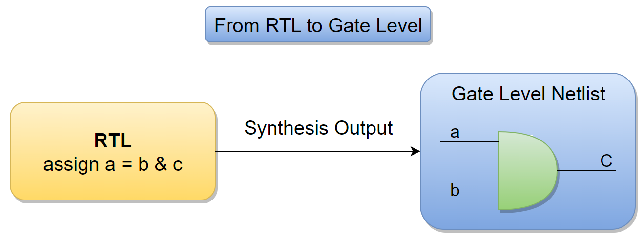
RTL Netlist: The process of converting the Higher Level Representation (RTL – Registor Transfer Level) into Lower Level Representation (Gate Level).

RTL Netlist vs Synthesized Netlist
The RTL code of design module is transformed into gate level netlist through the process of synthesis. Synthesis is the most curricular step in chip designing among all other steps. At the synthesis process one can visualize the designs which will appear after manufacturing. The functionality of a device written in a language such as verilog or VHDL is called RTL. If it can be synthesized to convert into gate level description. After synthesizing a RTL we get a netlist which is the gate level description of the device.
RTL Netlist or RTL Representation of the AND Gate – Input to the Synthesis:
module test_top(

input a,

 input b,

output wire c

);

assign c = a & b;

endmodule
Schematic Representation of the Gate Level Netlist – From RTL to Gate Level (Synthesis Output) :
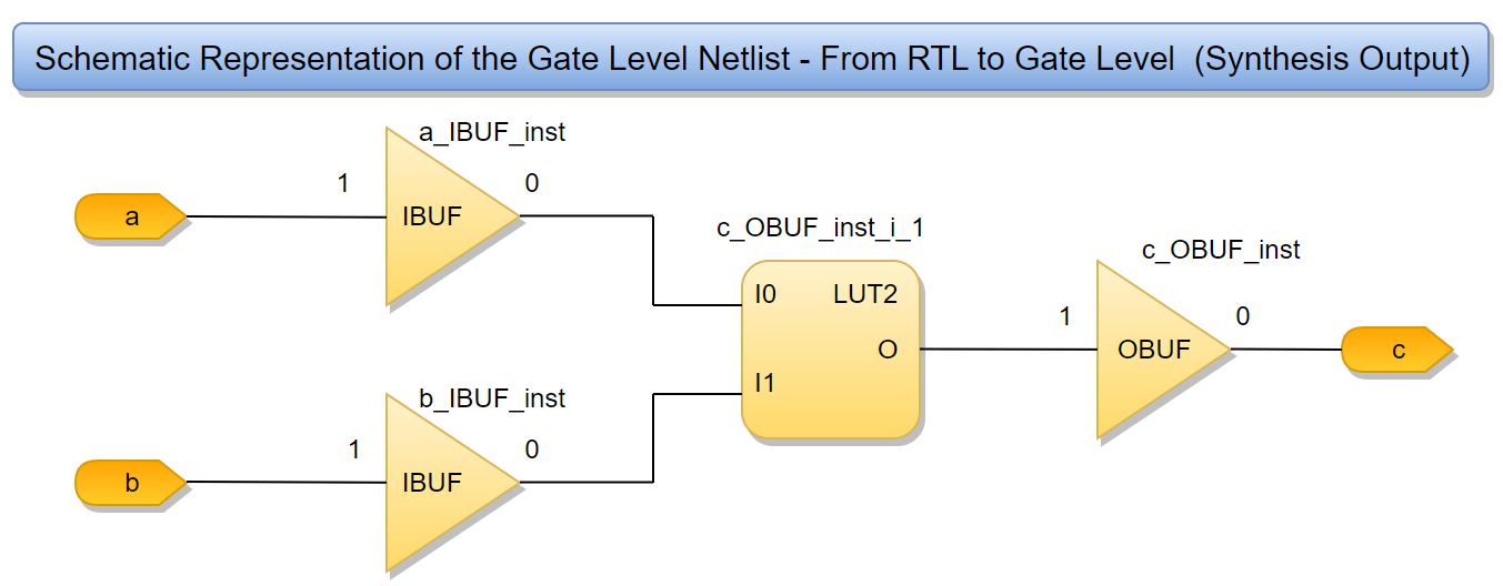
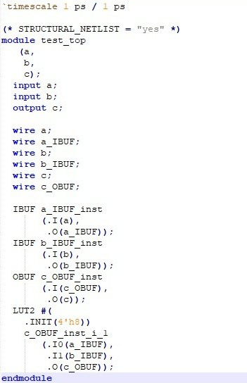
Netlist File Format in .v Generated by Synthesis Tool – Output or the Netlist Representation of the Synthesis Tool:
Figure: Netlist File Format Generated By Synthesis Tool
Developing a Gate Level Simulation Environment for verification of netlists:
It is assumed that RTL functional verification environment is already exist and now we need to upgrade the same environment for Gate Level Verification.
Gate level simulation is used to boost the confidence regarding implementation of a design and can help verify dynamic circuit behaviour, which cannot be verified accurately by static methods. It is a significant step in the verification process.
Gate level simulation overcomes the limitations of static-timing analysis and is increasing being used due to low power issues, complex timing checks at 40nm and below, design for test (DFT) insertion at gate level and low power considerations. For DFT, scan chains are inserted after the gate-level netlist is created; gate level simulation is often used to determine whether scan chains are correct.
Technology libraries at 45nm and below have far more timing checks and complex timing checks than older process nodes. Gate level simulation may take up to one-third of the simulation time and could potentially take most of the debugging time. It is run after RTL code is simulated and synthesized into a gate-level netlist. It requires a complete reset of the design.
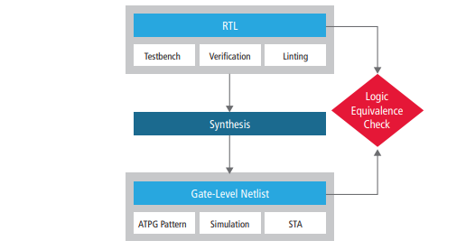
Reasons for running gate level simulation are reset verification, X optimism in RTL, timing verification on multi-cycle/asynchronous paths and basic heartbeat test.
Flat Level Netlist vs Hierarchical Netlist
Flat networks are designed to reduce the number of switches in a computer or design. It has a single device which connects the rest of the components. The debugging capacities are limited in a flat netlist, additionally synthesis tool can be used to optimize the circuit better. In a hierarchical design the design is separated using different switches. Moreover, the hierarchical network is separated into distinct layer switches each later performs a series of functions which defines its role in the network.
Hierarchical and Flat Synthesis
Hierarchical Synthesis
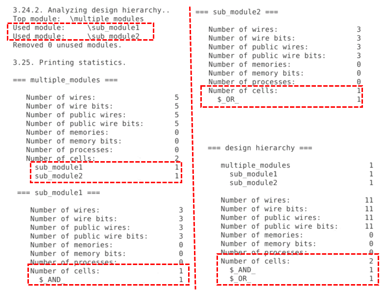
We have a RTL design where we have two sub modules, both instantiated inside top module as shown in below
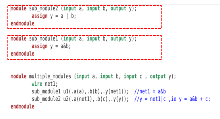
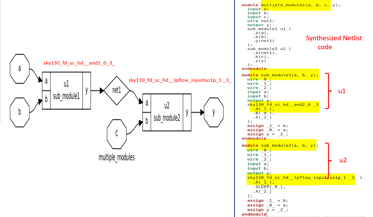
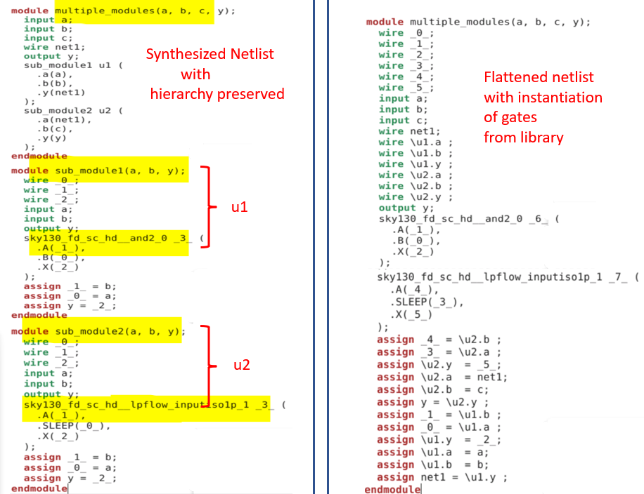
As per above RTL code we expect the netlist will consist of AND and OR gates from library. But lets see the synthesis result as shown below. We can see that synthesis has preserved the hierarchy as it uses sub-modules in place of gates in the design hierarchy of multiple modules a per below synthesis result.
To flatten the design yosys command Flatten is used. Flatten :This pass flattens the design by replacing cells by their implementation. This pass is very similar to the ‘techmap’ pass. The only difference is that this pass is using the current design as mapping Library/Cells and/or modules with the keep_hierarchy attribute set will not be flattened by this command.
After performing synthesis and generating netlist we will flatten the design to see if hierarchies are flatten out and gates are instantiated in netlist in place of submodules.
$ read_liberty -lib ../my_lib/lib/sky130_fd_sc_hd__tt_025C_1v80.lib
$ read_verilog multiple_modules.v
$ synth -top multiple_modules
$ abc -liberty ../my_lib/lib/sky130_fd_sc_hd__tt_025C_1v80.lib
$ write_verilog -noattr multiple_modules_hier.v			: to write hierarchical netlist
$ Flatten							: to flatten the design
$ write_verilog -noattr multiple_modules_Flat.v			: to write flattened netlist
Above image shows the difference between the Hierarchical and flatten netlist of Synthesis Output:
Verilog or RTL Code of the Logic Gates
Logic gates are the building block of digital circuit and system. We can make any digital circuit using logic gates. The are three basic logic gates AND, OR and NOT gate, two universal gate NAND and NOR and two other logic gates Ex-OR and EX-NOR. In this post, how to write Verilog code for logic gates is discussed.
There are 3 types of Verilog/RTL codes for each logic gate, you can use any of them:
- Uses Structural Modelling
- Uses Data Flow Modelling
- Uses Behavioral Modelling
NOT Gate
NOT gate has one input and one output and both are complement of each other. If input is 1 output is 0 and vice versa. The truth table of NOT gate is given below and we can write bolean expression of NOT gate as:
NOT Gate Truth Table
|
Input a |
Output y |
|
0 |
1 |
|
1 |
0 |
NOT Gate Verilog Code
//NOT gate using Structural modeling
module not_gate_s(a,y);
input a;
output y;

not(y,a);

endmodule
//NOT gate using data flow modeling
module not_gate_d(a,y);
input a;
output y;
assign y = ~a;
endmodule//NOT gate using behavioural modeling
module not_gate_b(a,y);
input a;
output reg y;
always @ (a)
y = ~a;
endmoduleNOT Gate Testbench
module not_gate_tb;
reg a;
wire y;

not_gate_s uut(a,y);

initial begin
a = 0;
#10
b = 1;
#10
$finish();
end

endmodule
OR Gate
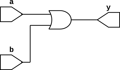
OR gate has many inputs (it can be two or more than two inputs) and one output. Output of the OR gate is 1 if one or more than one inputs are 1. The truth table of 2-input OR gate is given below and we can write boolean expression for OR gate as follows
y = a+b
OR Gate Truth Table
|
Input a |
Input b |
Output y
|
|
0 |
0 |
0 |
|
0 |
1 |
1 |
|
1 |
0 |
1 |
|
1 |
1 |
1 |
OR Gate Verilog Code
//OR gate using Structural modeling
module or_gate_s(a,b,y);
input a,b;
output y;

or(y,a,b);

endmodule
//OR gate using data flow modeling
module or_gate_d(a,b,y);
input a,b;
output y;
assign y = a | b;
endmodule//Not gate using behavioural modeling
module or_gate_b(a,b,y);
input a;
output y;
always @ (a,b)
y = a | b;
endmodule
OR Gate Testbench
module or_gate_tb;
reg a,b;
wire y;

or_gate_s uut(a,b,y);

initial begin
a = 0; b = 0;
#10
b = 0; b = 1;
#10
a = 1; b = 0;
#10
b = 1; b = 1;
#10
$finish();
end

endmodule
NOR Gate
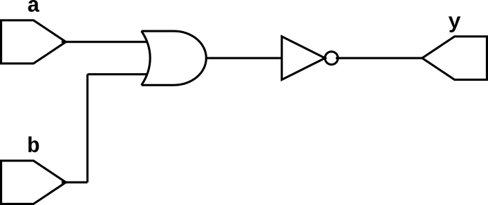
NOR gate has many inputs (it can be two or more than two inputs) and one output. It is NOR gate followed by NOT gate and output of the NOR gate is 1 if all inputs are 0 else it is 1. The truth table of 2-input NAND gate is given below and we can write boolean expression for OR gate as follows
NOR Gate Truth Table
|
Input a |
Input b |
Output y |
|
0 |
0 |
1 |
|
0 |
1 |
0 |
|
1 |
0 |
0 |
|
1 |
1 |
0 |
NOR Gate Verilog Code
//NOR gate using Structural modeling
module nor_gate_s(a,b,y);
input a,b;
output y;

nor(y,a,b);

endmodule
//NOR gate using data flow modeling
module nor_gate_d(a,b,y);
input a,b;
output y;
assign y = ~(a | b);
endmodule//NOR gate using behavioural modeling
module nor_gate_b(a,b,y);
input a;
output reg y; always @ (a,b) y = ~(a | b); endmoduleNOR Gate Testbench
module nor_gate_tb;
reg a,b;
wire y;

nor_gate_s uut(a,b,y);

initial begin
a = 0; b = 0;
#10
b = 0; b = 1;
#10
a = 1; b = 0;
#10
b = 1; b = 1;
#10
$finish();
end

endmodule
AND Gate
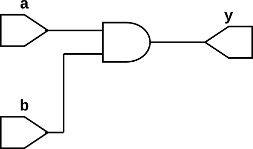
AND gate has many inputs (it can be two or more than two inputs) and one output. Output of the AND gate is 1 if and only if all of the inputs are 1. The truth table of 2-input AND gate is given below and we can write boolean expression for AND gate as follows
y = ab or y = a.b or y = a & b
AND Gate Truth Table
|
Input a |
Input b |
Output y |
|
0 |
0 |
0 |
|
0 |
1 |
0 |
|
1 |
0 |
0 |
|
1 |
1 |
1 |
AND Gate Verilog Code
//AND gate using Structural Modeling
module and_gate_s(a,b,y);
input a,b;
output y;

and(y,a,b);

endmodule
//AND gate using Data Flow Modeling
module and_gate_d(a,b,y);
input a,b;
output y;
assign y = a & b;
endmodule//AND gate using Behavioral Modeling
module nAND_gate_b(a,b,y);
input a;
output y;
always @ (a,b)
y = a & b;
endmoduleAND Gate Testbench
module and_gate_tb;
reg a,b;
wire y;

and_gate_s uut(a,b,y);

initial begin
a = 0; b = 0;
#10
b = 0; b = 1;
#10
a = 1; b = 0;
#10
b = 1; b = 1;
#10
$finish();
end

endmodule
NAND Gate
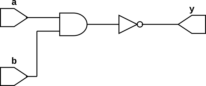
NAND gate has many inputs (it can be two or more than two inputs) and one output. It is AND gate followed by NOT gate and output of the NAND gate is 0 if all inputs are 1 else it is 1. The truth table of 2-input NAND gate is given below and we can write boolean expression for OR gate as follows:
NAND Gate Truth Table
|
Input a |
Input b |
Output y |
|
0 |
0 |
1 |
|
0 |
1 |
1 |
|
1 |
0 |
1 |
|
1 |
1 |
0 |
NAND Gate Verilog Code
//NAND gate using Structural modeling
module nand_gate_s(a,b,y);
input a,b;
output y;

nand(y,a,b);

endmodule
//NAND gate using data flow modeling
module nand_gate_d(a,b,y);
input a,b;
output y;
assign y = ~(a & b);
endmodule//NAND gate using behavioural modeling
module nand_gate_b(a,b,y);
input a;
output reg y;
always @ (a,b)
y = ~(a & b);
endmoduleNAND Gate Testbench
module nand_gate_tb;
reg a,b;
wire y;

nand_gate_s uut(a,b,y);

initial begin
a = 0; b = 0;
#10
b = 0; b = 1;
#10
a = 1; b = 0;
#10
b = 1; b = 1;
#10
$finish();
end

endmodule
Visit Silicon Synergy to know More
Explore our IC Design Courses in Analog IC Design, Digital Design & Verification

