VLSI Design Flow
VLSI(IC) Design Cycle
VLSI(IC) Design Flow: The process of designing, manufacturing, and testing ICs is complex and exhaustive. The main contributors are the design and verification teams, IP vendors, and IC manufacturers.
This article introduces the integrated circuit (IC) design cycle. It is intended for people who have recently joined the semiconductor/EDA industry. I couldn’t find a complete IC design cycle on the internet and hence I have written this.
What is Integrated Circuits (IC’s) ?
An integrated circuit, also called a chip, is an electronic circuit formed from thousands, millions, or even billions of transistors, resistors, and capacitors. It performs the same function as a larger circuit constructed using discrete (individually packaged) components, but an IC is an extremely compact device that is constructed as a single unit on a small piece of semiconducting material. The main raw material used in making an IC is silicon; hence the fact that ICs are popularly called “silicon chips.” Other raw materials like germanium and gallium arsenide may also be used, but silicon is the primary choice due to the following reasons:
- Silicon is a semiconductor, which means it can act as a conductor and insulator under certain conditions that is controlled in a process called as doping. Doping means adding impurities to alter the electrical properties of an element.
- Silicon is abundant on earth, which makes it very affordable.
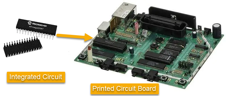
An IC is designed for a purpose and can be used across various industries, such as aerospace, automotive, telecom, computers, and so on. One or more ICs, along with other components and connectors, are mounted on the printed circuit board (PCBs) and connected with thin strips of copper to cater an application. A very common use of a PCB is as the mother board of a computer.
Picture: Integrated circuit (IC) and printed circuit board (PCB)
The entire process of designing, manufacturing, and testing an IC is quite complex. IC designers design and validate the ICs, while the IC manufacturers (often called the fab or foundry) fabricate and test the ICs. This article explains the end-to-end process of IC designing, manufacturing, and testing including the evolution IC’s in 75 years and also the type various of IC’s.
Evolution of Computer Chips and IC’s in 75 Years
There are 37.2 trillion cells in the human body. Yet, while the size of a single cell does not really need to change for the sake of humankind’s evolution. For robots to evolve, it is essential that the transistor, i.e., the robot cell, get smaller and smaller as possible.
1. In 1945, the first-ever invented computer, the ENIAC, had 18,000 vacuum tubes(old fashion transistors) in it, weighed 30 tons, and occupied 167 meters squared.
2. By 1948, the current type of transistor(the one that’s now just 3nm or 2nm) was invented, and it was 40 micrometers long (about 6,000 times longer than the current one).
3. In 1959, the integrated circuit puts the nearly 30-ton ENIAC(1947) on one tiny chip.
4. In 1971, the first-ever microprocessor 4004(the powerhouse of any electronic gadget) by Intel is released — The 4004 had 2,300 transistors.
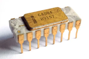
5. Back in 1977, Steve Jobs and Wazniak introduced the Apple II. revealing Apple’s first launch of a personal computer aimed at a consumer market. The transistor size was 5 micrometers
6. The year: 1987 — Transistor Size: 800 nanometers.
7. 10 years after the 68030 microprocessor featured 273,000 transistors came to the market with transistor size(800nm) that was below 1000 nanometers for the first time.
8. Only in 2004, Intel introduced the Pentium 4 with 112,000,000 transistors. And for the first time, the size of a single transistor was below 100 nanometers.
9. In 2007 Steve Jobs introduced the first iPhone; the touch screen or smart phone based on 45nm
10. In 2021, the transistor size further came down to 5 nanometers.
11. In 2023, the Apple released iPhone 15 Pro models that was powered by the A17 Pro processor, based on the the industry’s first 3-nanometer chip.
11. TSMC expects to create chip packages with over 1 trillion transistors by 2030
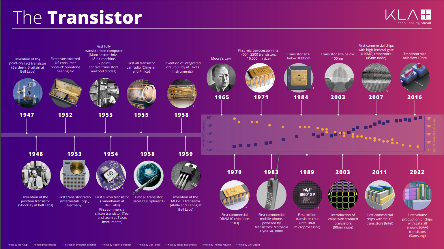
Picture Credit: https://www.kla.com
It is no secret that robots and AI are starting to replace humans in a few sectors nowadays.
Type of IC’s
The following figure illustrates the various type of ICs:
Picture: Various type of integrated circuits
1. ASIC (Application Specific Integrated Circuit)
An IC designed for a specific application is called an ASIC. The main characteristics of ASICs are as follows:
- Performs the same function throughout its life time
- Does not have a processor
- Design cycle is time-consuming and expensive
- Manufactured in higher volumes
- High speed and low power consumption
- Can be digital, analog, or both
Applications: Routers, switches, modems, etc.
2. ASSP (Application Specific Standard Part)
The characteristics of an ASSP are like those of an ASIC.
Applications: Ethernet controllers, PCIE controllers, USB interfaces, etc.
3. FPGA (Field Programmable Gate Array)
- Suitable for designs that need frequent customizations
- Does not have a processor
- Design cycle is not time-consuming and inexpensive
- Suitable for lower volume designs
- Lower speed and low power consumption
Applications: Prototyping ASICS or SoCs, device controllers, signal processing systems, image processing systems, etc.
4. SoC (System on Chip)
An ASIC or ASSP with a processor is an SoC, and hence the characteristics of an SoC are similar to those of an ASIC or ASSP.
Applications: Voice, video, and image signal processing, wireless communication, automobiles, etc.
5. Programmable SoC or SoC FPGA

- Suitable for designs that need frequent customizations with processing capabilities
- Smaller size
- Higher bandwidth communication between the processor and FPGA
- Design cycle is not time-consuming and inexpensive
- Lower risk as it is reprogrammable
- Lower speed and low power consumption
Applications: Networking, aerospace, defense, etc.
6. Microcontroller (µC or MCU)
- Compact, since all of the peripherals are present in the IC
- Has a processor
- Cheaper than microprocessors
- Lower speed and low power consumption
- Suitable for smaller designs as it is compact
- Performs less-complex tasks
Applications: Microwave ovens, washing machines, DVD players, mobiles, etc.
7. Microprocessor (µP or MPU)
- Expensive
- Higher speed and higher power consumption
- Suitable for larger designs
- Performs complex tasks
Applications: Desktop PC’s, laptops, notepads, automobiles, trains, etc.
The IC Design Cycle
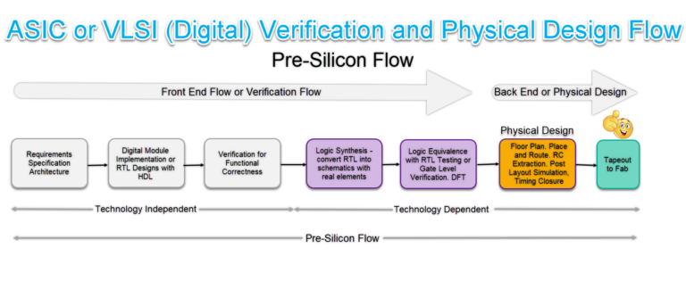
The illustration below reflects the IC design cycle or IC Design Flow(each step is explained in the following sections):
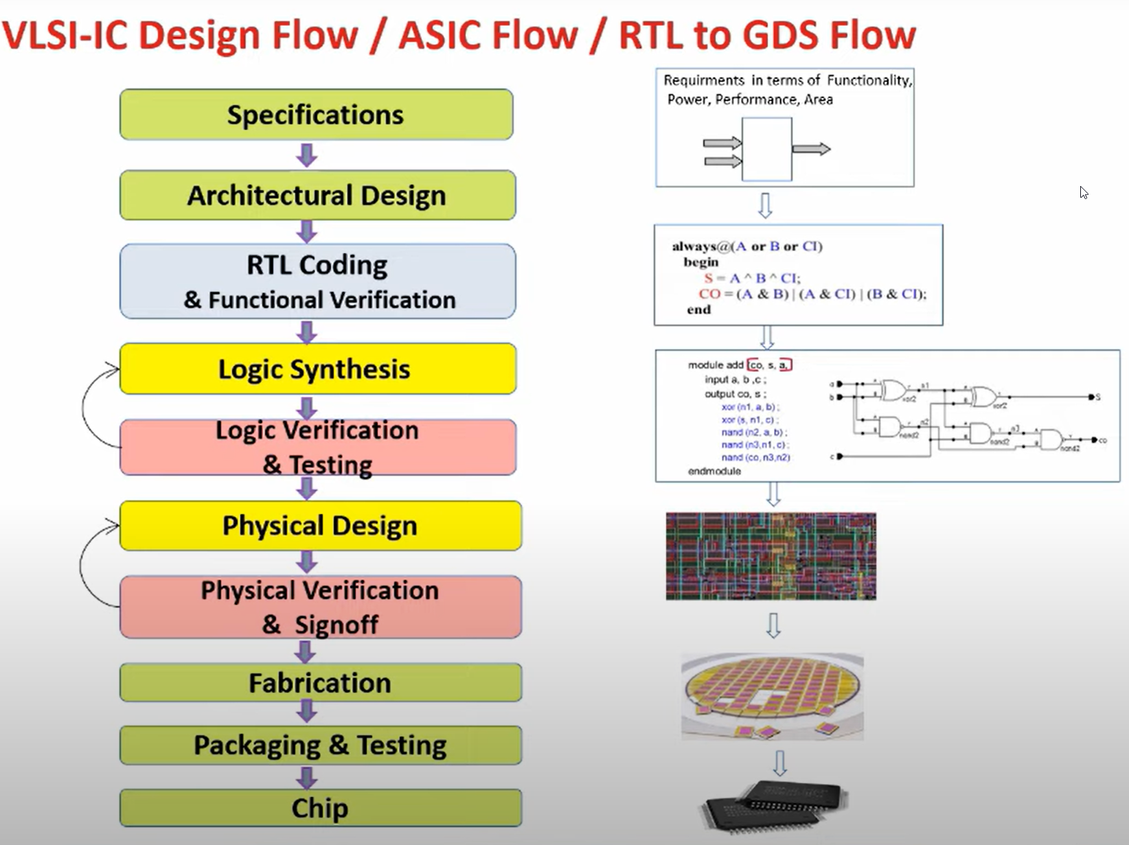
Picture: The IC Design Cycle
1. System Specification
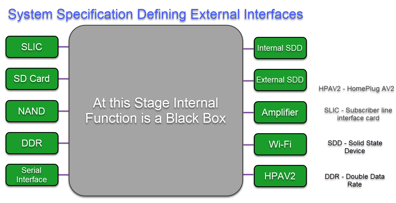
The first step in the ASIC design flow is to define the requirements of the chip. This involves understanding the application for which the chip is being designed, its performance requirements, power consumption, size, and other specifications. The IC vendors meet the potential customers to identify the features they are looking for and to prepare a list of functional requirements. System specification is the process of specifying the functional specifications (or requirements) of the system (IC) and defining its external interfaces.
Picture: System Specification: Defining the External Interfaces & Specifications
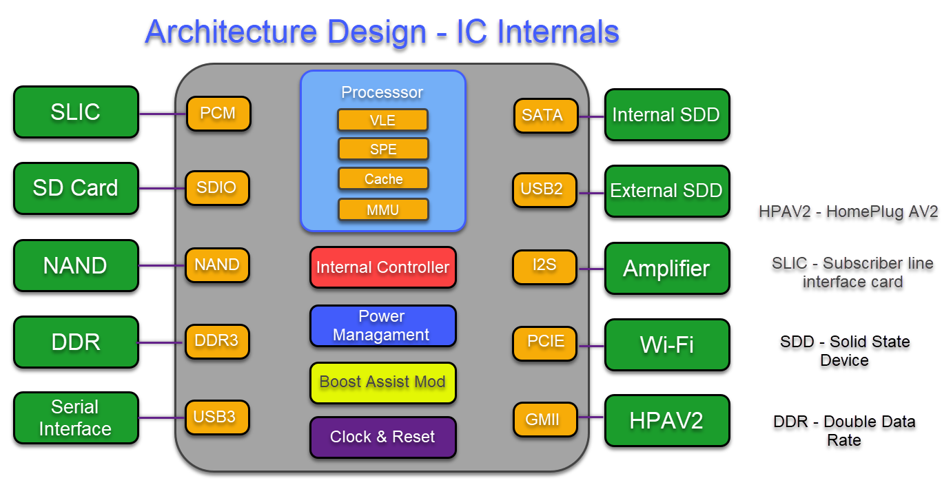
2. Architecture Design
Once the requirements are defined, the next step is to develop a high-level architecture for the chip. This involves identifying the major functional blocks of the chip, the interconnections between them, and the data flow through the chip. Also, includes creating or shopping the intellectual property (IP) blocks, and defining the software interfaces, timing, performance, area, and power constraints. Standard industry IP blocks are available from IP vendors etc. The design architecture of a product is similar to the block diagram of the product. The design architect develops the architecture. Microarchitecture functionalities such as hardware/software interfacing are defined at this stage.
Picture: IC’s Internal Architecture Design
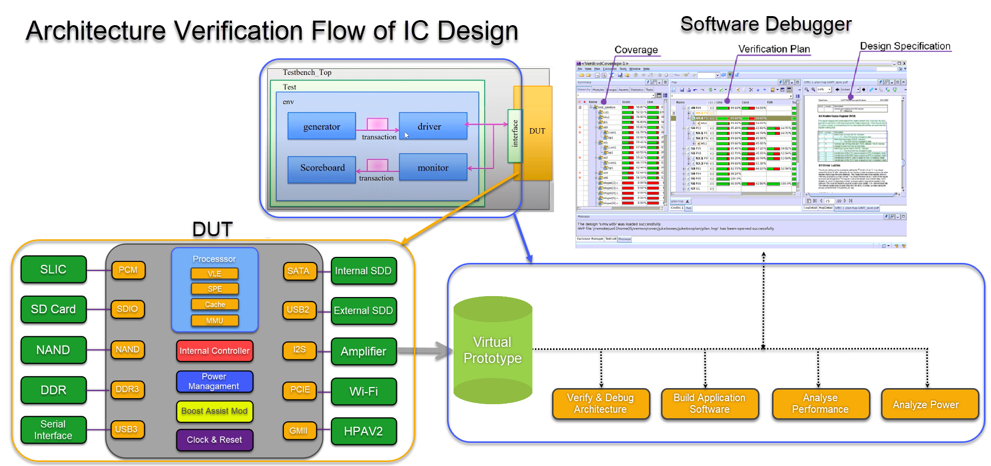
3. Architecture Verification
Architecture verification is the process of building a software version of the hardware system. This is created from functional models using high-level languages like C, C++, or SystemC or System Verilog. The architecture, performance, and power of the entire system are evaluated using software debuggers.
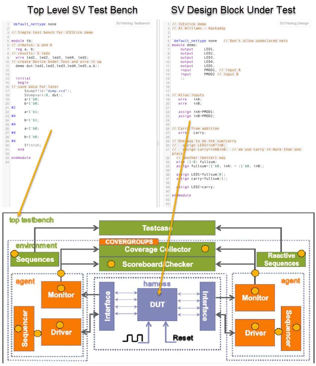
The first step in the verification process is to prepare a verification plan which is tightly coupled with the design specification that involves what all features need to be tested and techniques used to verify the design under test (DUT) such as scoreboard check planning, assertions, and functional coverage writing, etc. The test bench is a setup or environment that allows verification of DUT.
The test bench is responsible for:
1. Generating input stimulus
2. Driving an input stimulus
3. Monitor design activity at the output and input level.
4. Compare output transaction correctness based on the driven input stimulus.
5. Sampling function converges and assertion correctness.
Test bench consists of following components:
1. Transaction : The transaction is a packet that is driven to the DUT or monitored by the monitor as a pin-level activity. In simple terms, the transaction is a class that holds a structure that is used to communicate with DUT.
2. Generator: The generator creates or generates randomized transactions or stimuli and passes them to the driver
3. Driver : The driver interacts with DUT. It receives randomized transactions from the generator and drives them to the driven as a pin level activity.
4. Monitor : The monitor observes pin-level activity on the connected interface at the input and output of the design. This pin-level activity is converted into a transaction packet and sent to the scoreboard for checking purposes.
5. Agent : An agent is a container that holds the generator, driver, and monitor. This is helpful to have a structured hierarchy based on the protocol or interface requirement.
6. Scoreboard : The scoreboard receives the transaction packet from the monitor and compares it with the reference model. The reference module is written based on design specification understanding and design behavior.
7. Environment : An environment allows a well-mannered hierarchy and container for agents, scoreboards.
8. Testbench top : The test bench top is a top-level component that includes interface and DUT instances. It connects design with the testbench
9. Test : The test is at the top of the hierarchy that initiates the environment component construction and connection between them. It is also responsible for the testbench configuration and stimulus generation process
Picture: Architecture Verification
Formal Verification – Property Checking
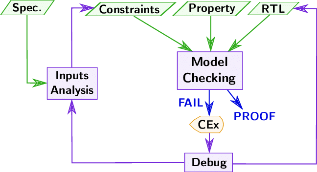
Formal verification is the process of verifying the correctness of the design statically employing mathematical methods and without using any stimulus or timing checks.
A formal verification method called property checking is used to prove that the implemented system model meets the design requirements (or specifications). In property checking, the system requirements are defined using property specification languages, such as PSL and SVA, and the mathematical model of the implemented system is created. The system requirements and the mathematical model are compared using a model checker to confirm that the system meets the requirements.
Picture: Formal Verification — Property Checking
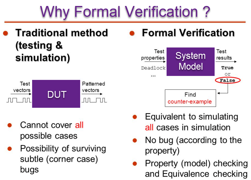
4. Formal Verification vs Functional Simulation
Formal Verification (a.k.a Formal, a.k.a FV) is a different style of verification but achieves the same end goal — weeding out bugs from your design. The testbench, constraints, checkers and coverage are written using System Verilog Assertions.
One of the big differences between Functional and Formal Verification is the role that the tool plays.
In Functional Simulation/Verification:
you write every piece of the testbench manually.
Testcase – You generate the stimulus and decide when it is injected into the RTL
Driver – You write the drivers or BFMs that do the injection of the stimulus based on a certain protocol
Monitor – You write the monitors that receive the output from the RTL
Model – You code a detailed reference model, a zero-time equivalent of the RTL, which produces a predicted result
Checkers – You write the checkers and scoreboard that compare the output from the RTL versus that from your reference model and declare Pass or Fail
You do all the work in Functional Verification. The testbench and tests orchestrate everything, and the tool merely simulates on a clock-by-clock basis what’s happening in the RTL as you inject the desired stimulus. Also, a lot of code needs to be written before you can write your first test.
In Formal Verification:
the tool does a lot of the heavy lifting. There is no concept of driver, monitor or test cases.
Here are the main features in Formal Verification:
1. The inputs or internal variables of the DUT are constrained according to the design specification using SVA assume directive
2. Checkers are written on the desired outputs, or internal variables of the DUT, using SVA assert directive
3. SVA cover property is used to collect functional coverage
4. You could also write small pieces of modeling code which are just sufficient for a particular checker. This is different from Functional Simulation where you write a detailed reference model of the block you are verifying.
5. Design Entry with Behavioral Module
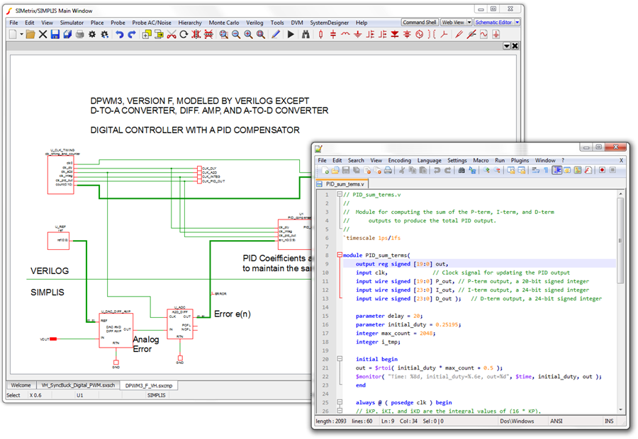
After the architecture of the system has been designed and verified, the next step is design entry. This is the process of capturing the complete system design using hardware design languages (HDLs), such as Verilog, System Verilog, VHDL, Verilog-AMS(For Mixed Signal Behavior), Wreal, VerilogA (For Analog Behavior) and/or Schematic captures with MOSFET models to simulate along with Digital and/or Analog/Mixed-Signal simulators in the design environments. Most of time designers use EDA tools to enter or add the designs/schematics including simulation and verify the results using EDA tools from Cadence, Synopsys or Siemens(Formerly Mentor Graphics) The design contains the details of the IC input and output pins, IP block instantiations, design connectivity, clock and reset strategy, and so on.
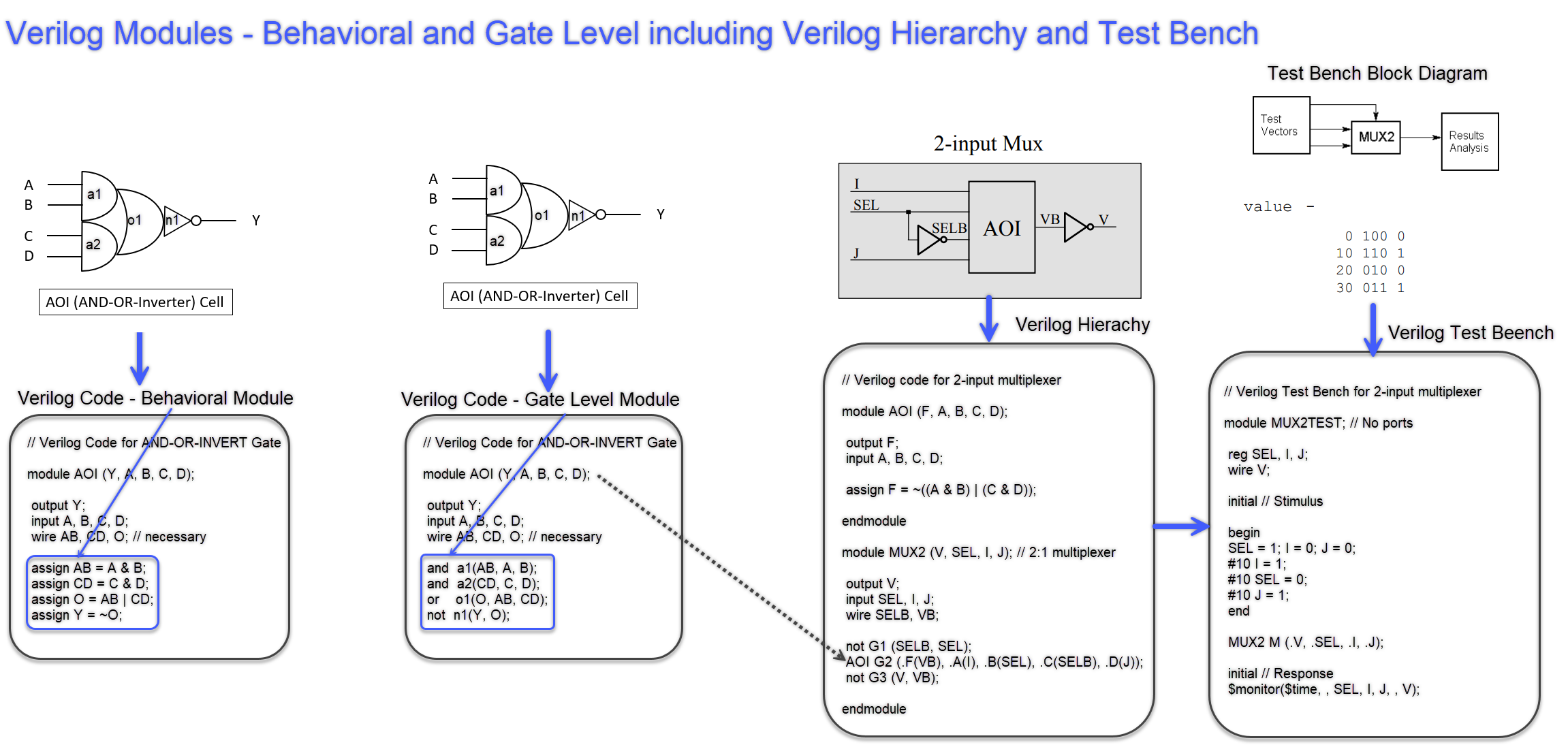
A Simple Behavioral Description of the Verilog Module Design
A design is described in Verilog using the concept of a module. A module can be conceptualized as consisting of two parts, the port declarations and the module body. The port declarations represent the external interface to the module. The module body represents the internal description of the module – its behaviour, its structure, or a mixture of both. Let’s imagine we want to describe an and-or-invert (AOI) gate in Verilog.
Verilog Module of an AOI Gate
// Verilog code for AND-OR-INVERT gate
module AOI (input A, B, C, D, output F);
assign F = ~((A & B) | (C & D));
endmodule
// end of Verilog code
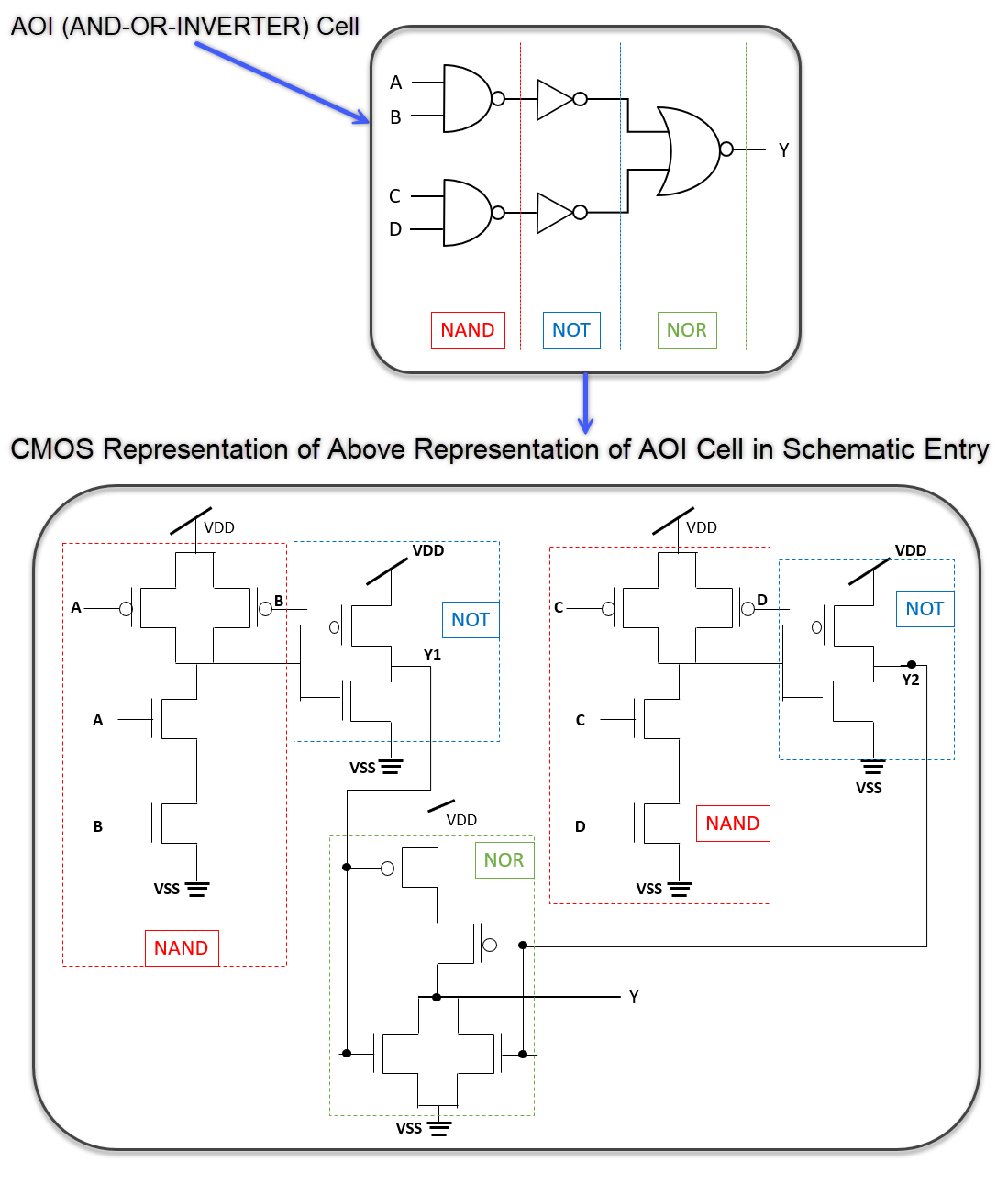
CMOS Representation of AOI Gate/Cell entry in Schematic Editor
EDA Tool Environment for the Simulation
Picture: Design Entry with Behavioral Verilog Module
6. Functional Simulation of the Modules
Functional simulation is the process of verifying the functional behavior of the design using a software simulator. This does not consider the timing delays of the design elements. It verifies the IC level connectivity, IP blocks in the IC-level environment (generally, IP blocks are pre-verified), end-to-end functional paths, pad connectivity, inter-module interaction, external module interaction, and so on.
The test bench is a set of codes that check whether (or not) the RTL implementation meets the design specification. It embodies both valid and expected conditions, along with invalid and unexpected conditions, to check that the design functions as intended.
Picture: Functional Simulation
7. Formal Verification – Equivalence Checking
As we noted earlier, formal verification is the process of verifying the correctness of the design statically employing mathematical methods and without using any stimulus or timing checks.
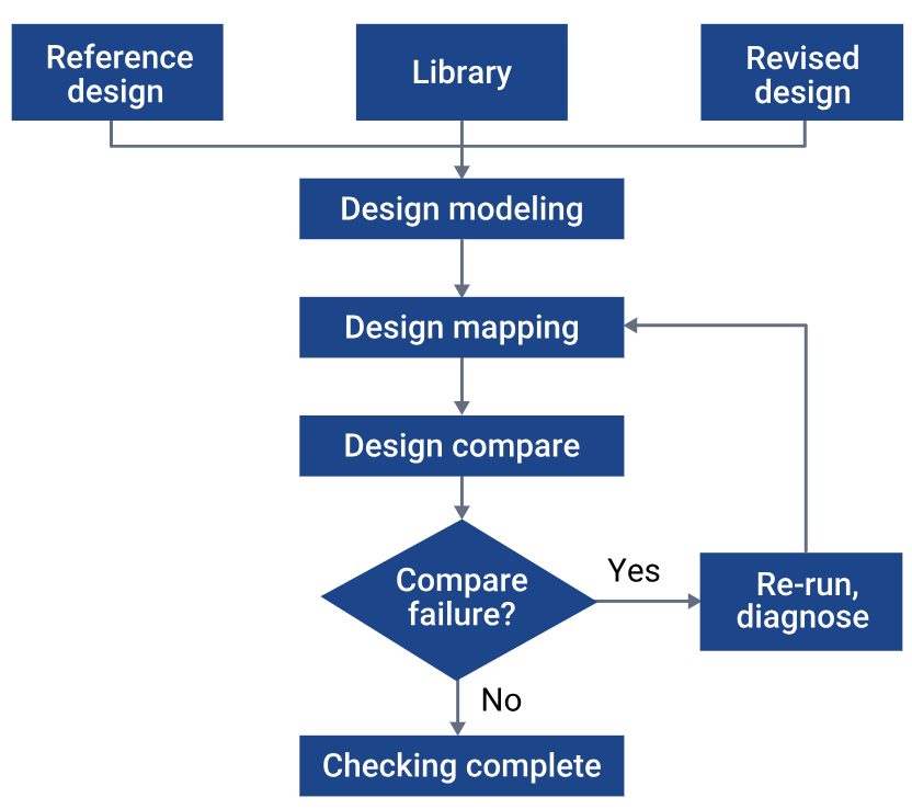
There are three basic steps in equivalence checking:
1. Setup
2. Mapping
3. Compare
Inputs to Setup include the verified reference design, library elements and the revised design. In this step the inputs are read in and data structures are created to facilitate the subsequent steps.
In Mapping, key points of the design are mapped and compared. Logic cones are typically used to organize compare points. A logic cone is a block of combinational logic that drives a compare point. Inputs to a logic cone include register output pins, primary input ports and black-box output pins. Compare points include registers, primary output ports and black-box input pins.
During Compare, the key mapped points are examined to determine if they are equivalent, non-equivalent, or inverted equivalent. Parts of the design that return an inconclusive result can be rerun with a higher level of effort to resolve.
A formal verification method is also called equivalence checking is used to find the functional equivalence of a design by comparing it with the golden design.
Picture: Formal Verification — Equivalence Checking in IC Design Flow(Source: Synopsys)
8. Pre-Silicon Validation
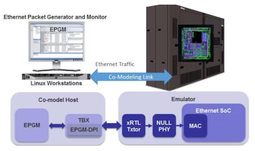
Pre-silicon validation is the process of verifying the design in hardware before sending it for manufacturing. It validates high-risk or newly-developed IPs and saves cost on re-spinning ICs. Pre-silicon validation can be performed using either an emulator or an FPGA. During the pre-silicon process, engineers test devices in a virtual environment with sophisticated simulation, emulation, and formal verification tools. In contrast, post-silicon validation tests occur on actual devices running at-speed in commercial, real-world system boards using logic analyzer and assertion-based tools. Some companies (like Intel) uses pre-silicon validation to refer to verification which is really verifying the design before tapeout / silicon fabrication.
Advantages:
- Very fast compared to the simulation environment
- Can probe a limited set of internal signals for debugging
- Software and application-level scenarios can be validated ahead of tapeout
Limitations:
- The hardware is expensive
- Analog IP blocks cannot be validated
- System clock speed is slower compared to that on the real silicon
- Requires multiple hardware setups, especially if validation and software teams are spread across multiple geographical locations
9. Emulation in IC Design Flow
Emulation is the process of verifying the functionality of the system on a hardware device called an emulator. An emulator can run a very large IC design much faster than simulation and can run many IC designs simultaneously at various clock speeds. The following photo shows a state-of-the-art emulator:
Picture: Emulator (Source: Siemens)
10. FPGA-Based Prototyping
FPGA-based prototyping is the process of verifying the functionality of the system using one or more FPGAs. The following steps are followed for FPGA prototyping:
1. The ASIC RTL (register transfer level) code is converted to FPGA RTL code. It includes using different memories, removing analog blocks, rewriting the clocking scheme, and so on.
2. If the complete FPGA RTL code doesn’t fit into single FPGA then the code is partitioned into multiple FPGAs.
3. FPGA tools are used for synthesis and place-and-route.
4. The bit file is downloaded into the FPGA and the design is verified.
Picture: FPGA-Based Prototyping (Credit: semiwiki.com)
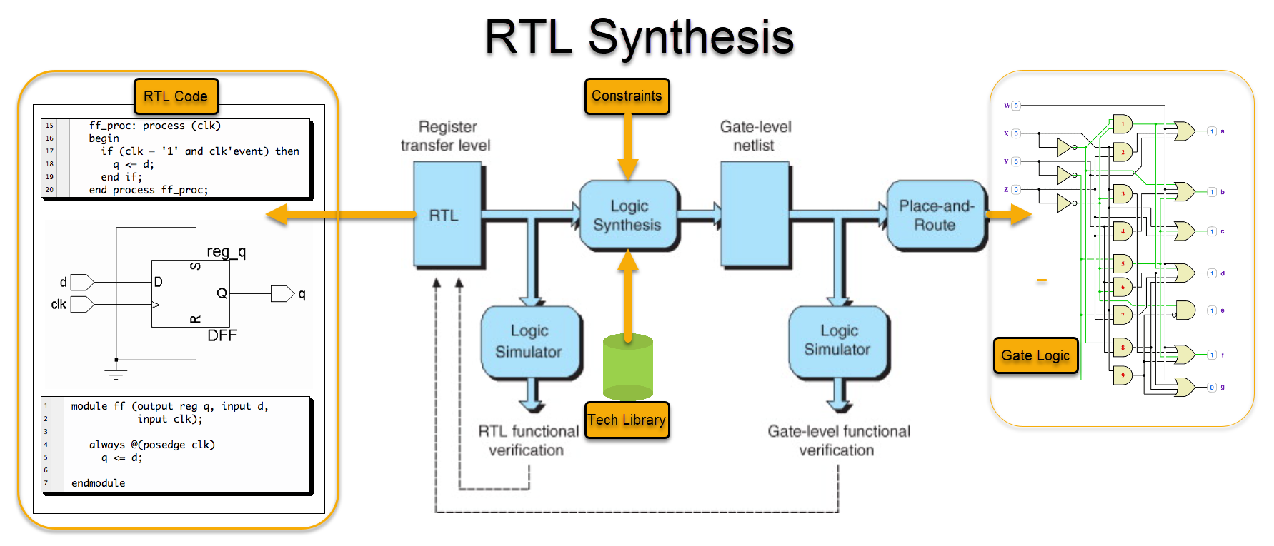
11. RTL Synthesis
Once the RTL design is verified, it is synthesized to create a gate-level netlist. Synthesis is the process of converting the design’s RTL code into an optimized gate-level representation, given a technology library and design constraints. The following steps are performed in synthesis:
1. Translation: The design RTL code is translated into a technology-independent Boolean equation.
2. Optimization: The Boolean equation is optimized, and any redundant logic is removed.
3. Technology Mapping: The technology independent Boolean equation is mapped to the technology-dependent logic gates with the help of the design constraints and the technology library.
Picture: RTL Synthesis in IC Design Flow
12. Static Timing Analysis (STA)
Static timing analysis (STA) is the process of verifying the timing characteristics of a design without providing any stimulus. STA is fast and exhaustive, but it doesn’t check the functionality of the design. An electronic device is driven by a clock signal; hence, it is imperative to verify that the design works at the specified clock frequency. STA is performed at various stages of the IC design cycle.
Picture: Static Timing Analysis (STA) in IC Design Flow
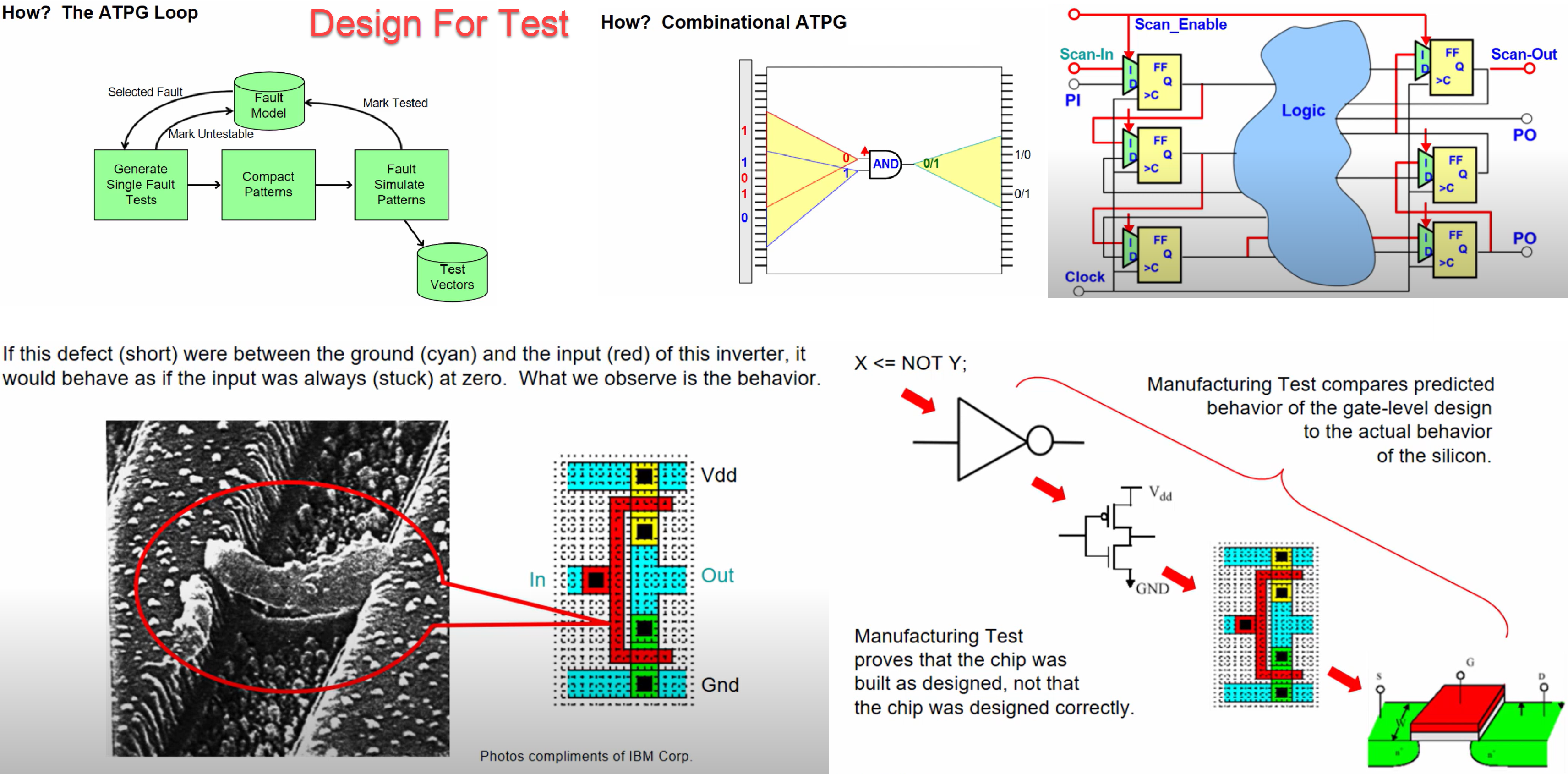
13. Design For Test (DFT)
The process of manufacturing an IC is not 100% error-free. Hence, extra logic, known as Design for Test (DFT) logic, has to be inserted in the design to aid in post-production testing of the IC to identify manufacturing defects. When an IC is manufactured, it is first checked for any manufacturing defects with the help of the DFT logic. If there are no manufacturing defects, then the IC is checked for functional correctness.
Picture: Design For Test in IC Design Flow(Source: https://Cadence.com YouTube Clips)
14. Pre-layout Gate Level Simulation (GLS)
Before the gate-level netlist is sent for physical layout, it is verified for functional and timing behavior by software applications. This is called pre-layout simulation or Gate Level Simulation (GLS).
Simulations are an important part of the verification cycle in the process of hardware designing. It can be performed at varying degrees of physical abstraction:
1. Transistor level
2. Gate level
3. Register transfer level (RTL)
In many companies RTL simulations is the basic requirement to signoff design cycle, but lately there is an increasing trend in the industry to run gate level simulations (GLS) before going into the last stage of chip manufacturing. Improvements in static verification tools like Static timing analysis (STA) and Equivalence Checking (EC) have leveraged GLS to some extent but so far none of the tools have been able to completely remove it. GLS still remains a significant step of the verification cycle footprint.
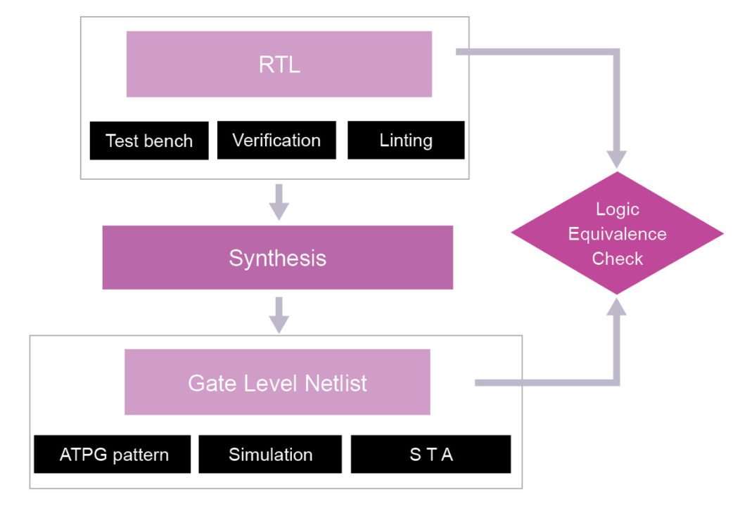
Firstly, let us look at the reasons why GLS is still used in the industry despite all the challenges associated with its execution.
The main reasons for running GLS are as follows
1. To verify the power up and reset operation of the design and also to check that the design does not have any unintentional dependencies on initial conditions.
2. To give confidence in verification of low power structures, absent in RTL and added during synthesis.
3. It is a probable method to catch multicycle paths if tests exercising them are available.
4. Power estimation is done on netlist for the power numbers.
5. To verify DFT structures absent in RTL and added during or after synthesis. Scan chains are generally inserted after the gate level netlist has been created. Hence, gate level simulations are often used to determine whether scan chains are correct. GLS is also required to simulate ATPG patterns.
6. Tester patterns (patterns to screen parts for functional or structural defects on tester) simulations are done on gate level netlist.
7. To help reveal glitches on edge sensitive signals due to combination logic. Using both worst and best-case timing may be necessary.
8. It is a probable method to check the critical timing paths of asynchronous designs that are skipped by STA.
9. To avoid simulation artifacts that can mask bugs at RTL level (because of no delays at RTL level).
10. Could give insight to constructs that can cause simulation-synthesis mismatch and can cause issues at the netlist level.
11. To check special logic circuits and design topology that may include feedback and/or initial state considerations, or circuit tricks. If a designer is concerned about some logic then this is good candidate for gate simulation. Typically, it is a good idea to check reset circuits in gate simulation. Also, to check if we have any uninitialized logic in the design which is not intended and can cause issues on silicon.
12. To check if design works at the desired frequency with actual delays in place.
13. It is a probable method to find out the need for synchronizers if absent in design. It will cause “x” propagation on timing violation on that flop.
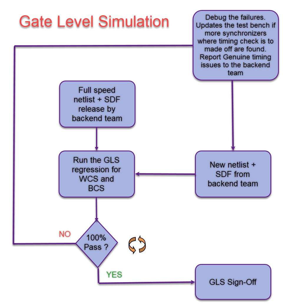
Execution strategy for GLS
Picture: The above diagram shows the GLS sign off flow
1. Planning the test-suite wisely to be run in GLS
In highly integrated products it is not possible to run gate simulation for all the SoC tests due to the simulation and debug time required .Therefore, the list of vectors which are to be run in GLS has be selected judiciously. The possible candidates for this list are:
1.1 Testcases involving initialization, boot up.
1.2 All the blocks of the design must have at least one testcase for GLS.
1.3 Testcases checking clock source switching.
1.4 Cases checking clock frequency scaling.
1.5 Asynchronous paths in the design.
1.6 Testcases which check entry/exit from different modes of the design.
1.7 Dedicated tests for timing exceptions in the STA.
1.8 Patterns covering multi clock domain paths in the design
1.9 Multi reset patterns are a good candidate for GLS
1.10 It must also be made sure that the test cases selected to be run in GLS are targeting the maximum desired operating frequency of the design. Should there be no time constraints, all tests run in RTL simulations can be rerun in GLS. Also, if there are no tests fulfilling the criteria mentioned above, then they should be coded.
2. Preserving design signals
Some signals which are critical for GLS debug can be preserved while synthesis.
3. Testbench updates for GLS
A list of all the synchronizer flops is generated using CDC tools. Also, other known asynchronous paths where timing checks needs to be turned off are analyzed and complete list of such flops is prepared which also includes reset synchronizers. The timing checks are turned off on all such flops to avoid any redundant debugging, otherwise they will cause “x” corruption in GLS. This work should be ideally done before the SDF arrives. It may happen that the name of the synchronizers in RTL and the netlist are different. All such flops should be updated as per netlist .Also, the correct standard cell libraries, correct models of analog blocks, etc. need to be picked for GLS.
4. Initialization of non resettable flops in the design
One of the main challenges in GLS is the “x” propagation debug. X corruption may be caused by a number of reasons such as timing violations, uninitialized memory and non resettable flops . There are uninitialized flops in design which by architecture are guaranteed to not cause any problems (if they settle to any value at start). Thus, there is a need to find out all such flops in the design (which are reviewed with designers) and initialize them to some random value (either 0 or 1) so as to mimic silicon.
5. Unit delay GLS for testbench cleanup
This step is not compulsory but is generally very fruitful if employed in the GLS execution. The setup is done for unit delay GLS (no SDF) and the testcases that are planned to be run on gate level are run with this setup to clean the testbench. This is done because the unit delay simulations are relatively faster (than those with SDF) and all the testbench/testcase related issues can be resolved here (for example – change probed logic hierarchy from RTL to gate, wrong flow of testcase, use of uninitialized variables in the testcases that can cause corruption when read via core, etc). Running the unit delay GLS is recommended because one can catch most of the testbench/testcase issues before the arrival of SDF. After the SDF arrives, focus should be more on finding the real design/timing issues, so we need to make sure that the time does not get wasted in debugging the testcase related issues at that time.6. Annotation warnings cleanup on SDF
When the SDF is delivered to verification team, then the simulations are run with the SDF/netlist. Specific tool switches need to be passed which picks us the SDF and tries to annotate the delays mentioned in the SDF to the corresponding instances/arcs in the netlist. This is known as “back-annotation.”
During this process, many annotation warnings are encountered which need to be analyzed and either sorted out or waived off by the design team. Most important warnings which need to be looked into are the ones which are due to non-existent paths i.e. the SDF has an arc but netlist does not have it. Also, there can be mismatch between the simulation model “specify” block and .lib of the IP.
6. Running GLS with SDF
(a) Early SDF (for initial debug)
This step involves use of a sdf in which timing is met at a lower frequency than target and GLS can be run at that frequency. This helps in cleaning up the flow and finding certain issues before the final SDF arrives.
(b) Full speed SDF (WCS and BCS)
This step starts with the sdf in which timing is met at target frequency. The entire setup is done and the planned pattern-suite is run on this setup and failures needs to be debugged according to a priority list which should be made before hand. All the high priority patterns need to be debugged first.
All issues found are discussed with the design and timing team and the required fixes are done in the netlist/SDF. This process is repeated until the GLS regression is clean on the final SDF
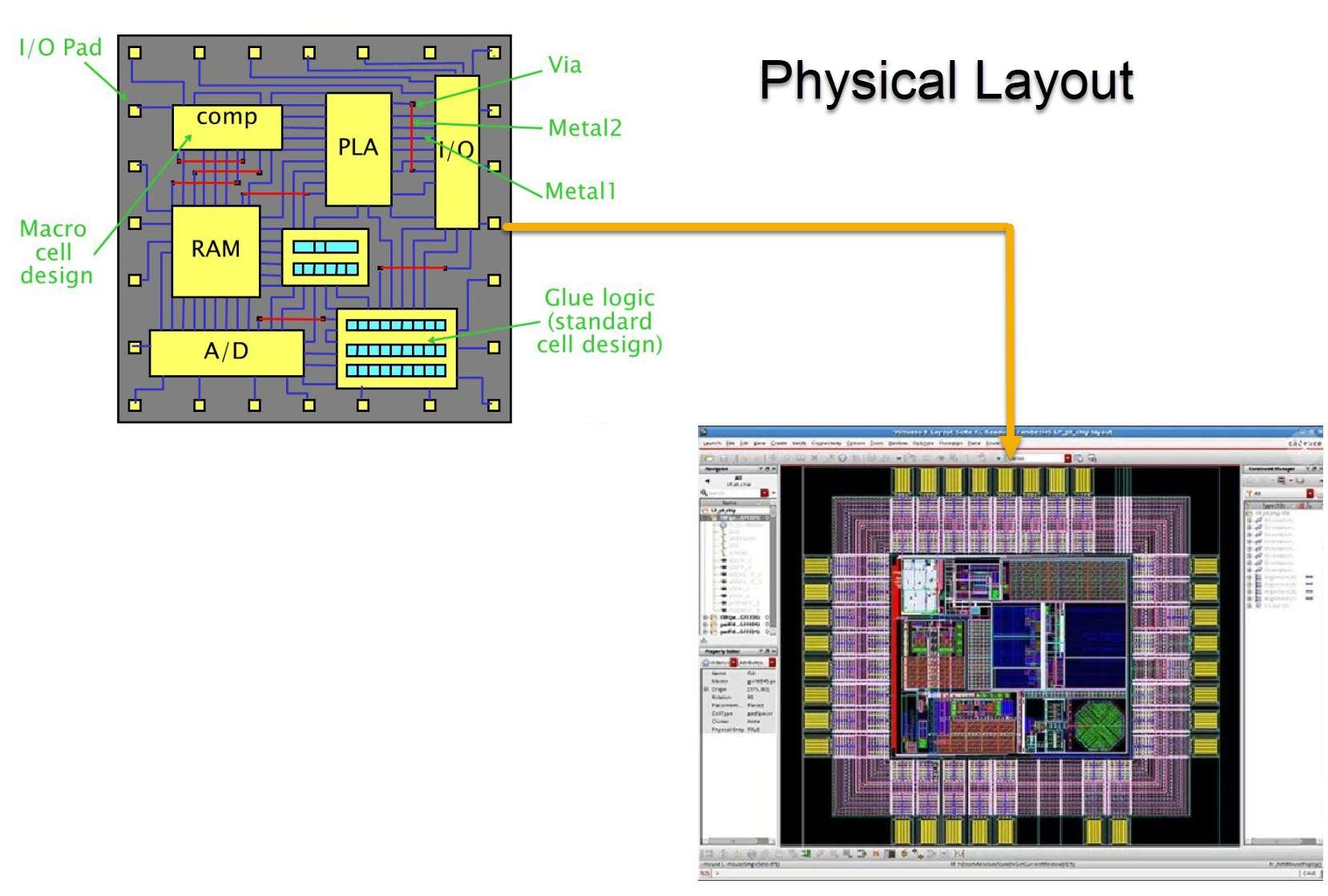
15. Physical Layout
Physical layout is the transition from the logical view of the IC to the physical view. The output of the physical layout process is a Graphical Database System (GDSII) file, which is a binary file format representing planar geometrical shapes, text labels, and other information related to the physical layout. The steps performed in physical layout are in brief below:
- Floor Planning: The major design blocks are identified, and space is allotted such that they meet the timing, area, and performance criteria. The IP structure, aspect ratio, and routing possibilities are also decided here.
- Partitioning: The IC is divided into functional blocks to make placement and routing easier.
- Place-and-Route: The design blocks are placed and connected such that there are no design rule violations.
- Clock Tree Synthesis: The clock is evenly distributed to all sequential elements in the design.
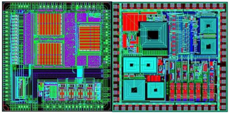
Picture: Physical Layout (Source: Cadence)
The detailed steps involved in the physical design process are outlined below, along with a typical back-end flow process.
1. Partitioning:
The physical design process starts with creating the netlist. The next step is called partitioning. Partitioning involves dividing the chip into smaller blocks. It can be described as decomposing a complex system into smaller sub-modules to satisfy the packaging constraints. It is done to simplify the placement and routing process. The output at the end of this step will be a set of sub-circuits having the functionality of the original circuit.
Partitioning helps in minimizing the length of global wires, which in turn decreases the size of the chip. Partitioning can be done at three levels, namely system-level, board-level, and chip level.
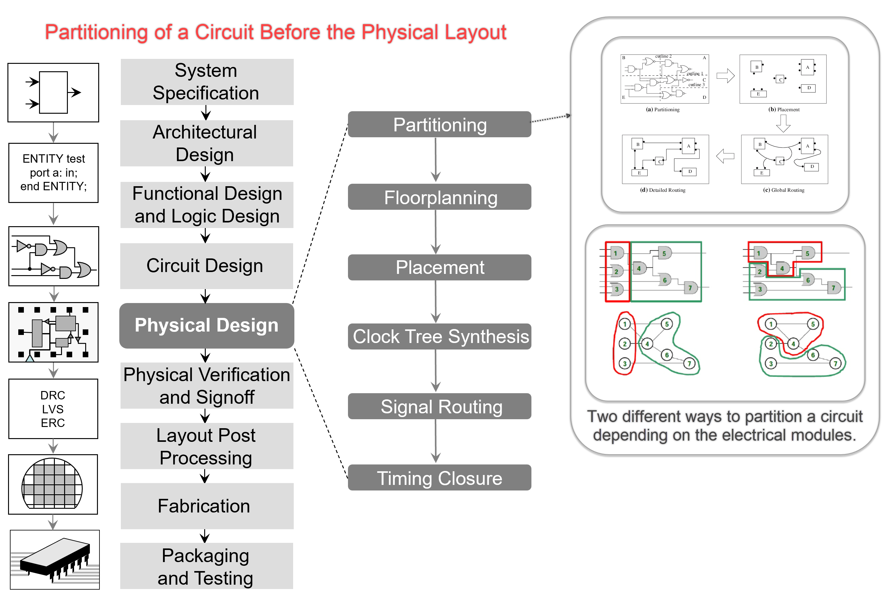
Picture: Example of Partitioning (Source: Research Gate and Wiki)
Incorrect partitioning can lead to an increase in delay. Partitioning can be done in two ways: Constructive or iterative and deterministic or probabilistic.
2. Floor Planning:
As the name suggests, floor planning is the process of determining structures that should be placed near each other. Space should be allocated to meet the space availability, performance expectations. It should not increase the area of the chip, as this increases the cost. It also takes into account the design IP cores’ placement needs. IO pins are also placed on the physical chip at this step.
The trade-off between speed and area is the most challenging aspect. This occurs due to the limited availability of routing resources. An increase in resources used leads to a decrease in the speed of operation. The data path section is given priority over non-structured logic. Data path includes modules like adders, subtractors, counters, and multiplexers.
If a floorplan is not executed correctly, it can lead to congestion in routing and wastage of die.
3. Placement :
In placement, gates in the netlist are assigned non-overlapping spaces on the die. Incorrect placement can affect the performance of the chip and even render it not fit for manufacturing. Placement uses RC values to calculate delay. All the wire load modules are removed in this step.
Placement is performed in the following steps:
3.1 Pre-placement: This step can downsize the cells being placed by collapsing the high-fanout cells. Fan-out refers to the number of outputs one cell can have. In short, optimization of the netlist is done at this step.
Insertion of spare cells, adding of special cells, and insertion of decoupling capacitors is done at this stage.
3.2 Optimization during placement: The Placement & Routing (PnR) tool is used for determining an approximate location for all of the cells. The tools optimize placement as per the timing constraints and congestion.
3.3 Post Placement optimization before Clock Tree Synthesis: In this step, the netlist is optimized with ideal clocks. It fixes critical timing violations like setup time and hold time violations. These violations can lead to a condition called metastability in which the flip-flop is at an unknown state. If these violations are not cleared, the chip does not function as desired. Global routing is used for placement optimization.
3.4 Post Placement optimization after Clock Tree Synthesis: It attempts to preserve clock skew. Clock skew occurs in synchronous (clock-based) circuits wherein the source clock reaches different flops at different times. Clock skew is classified as positive and negative skew, depending on if the clock is received before or after the expected time.
4. Clock Tree Synthesis (CTS):
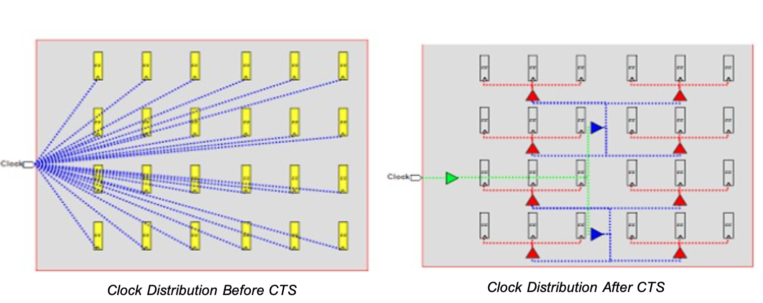
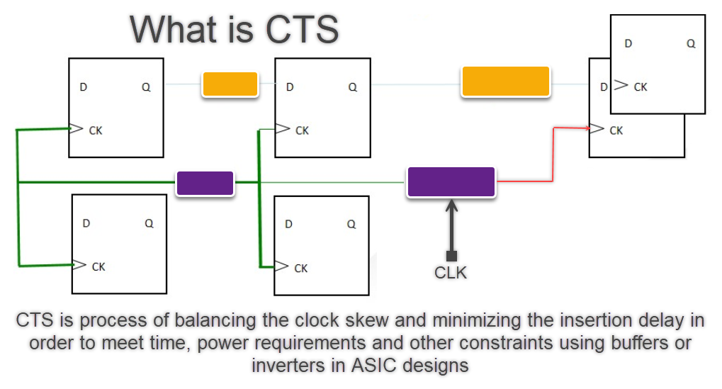
CTS is the process of even distribution of clock to all sequential elements on the chip. The primary purpose is to minimize the effects of clock skew and delay. Before CTS, all sequential elements are driven by a single clock. Buffers or inverters are added to the clock path of the design to achieve balanced or minimum skew. In an IC, the clock accounts for over half of the power consumption. Hence, it must be optimized.
What is CTS and Why
- Within most VLSI circuits, data transfer between sequential elements is synchronized by the processing clock
- Before CTS, all clock pins are driven by a single clock source having high fan-out and high load.
- CTS is the process of inserting buffers/inverters along the clock path of the ASIC or VLSI design to balance the clock delay to all clock inputs.
- In order to balance the skew and minimize insertion delay, CTS is performed.
Clock Distribution Before and After (Inserting Buffers) CTS
5. Signal Routing:
In signal routing, interconnections are made for each net by determining a precise path for every net. It creates wires to connect the properly placed components while obeying the design rules. Routing is done using EDA tools called routers. Routers aim to connect every pin to its associated terminals without leaving any pin open or creating a short. The router needs to ensure that the design meets the timing constraints. It cannot cross the area of design.
6. Timing Closure:
Violations related to timing (performance), noise (signal integrity), and design for manufacturability (yield) are removed.
Timing analysis can be done using either Static Timing Analysis (STA) or Dynamic Timing Analysis. STA checks whether a chip meets the timing constraints without simulating the design; it does not check the asynchronous part of the design. The basic timing violations are setup time and hold time violations. STA is performed using EDA tools built explicitly for this purpose.
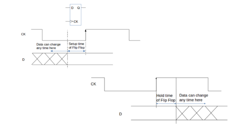
6.1 Set-Up Time Violation: Set-up time is defined as the time before a clock edge during which data must be stable. If the data reaches later, then it is called setup time violation. This is also called maximum time violation. This violation is usually solved by removing delay elements like inverters or buffers along the data path or clock path.
6.2 Hold Time Violation: Hold time is defined as the time after a clock edge for which data must be stable. If the data reaches earlier, then it is called hold time violation. This is also called minimum time violation. Hold time violation occurs when the data path is faster than the clock path. Hold time violation is solved by removing delay elements along the data or clock path.
The following images show the concept of setup and hold time and violations between two flip-flops.


Maximum Clock Frequency = 1/minimum clock period
The minimum clock period is the sum of delay times along the critical path, consisting of gate delay and interconnect delay. Interconnect delay is due to the R-C wire connections, and gate delay depends on multiple factors like fan-in, the logic used, and fan-out of the gate.
16. Post-Layout Simulation
Post-layout simulation is the process of verifying the design after the physical layout of the design has been established. Once the physical design is verified, the final design data is sent to the foundry for manufacturing. This stage is called tape out, and it involves creating the photomasks required for the fabrication process. The checks performed in post-layout simulation are as follows:
- Design Rule Check (DRC): The layout satisfies a set of rules required for manufacturing
- Electrical Rule Check (ERC): The layout satisfies a set of electrical design rules
- Layout vs. Schematic (LVS): The layout is functionally the same as the netlist of the design
Picture: Post-Layout Simulation in IC Design Flow
17. IC Fabrication
After post-layout simulation, the layout netlist in the form of a GDSII file, is provided to the IC manufacturer (foundry). The process of providing the GDSII file to the foundry is called tapeout. The IC fabrication process is illustrated below:
Picture: The IC Fabrication Process IC Design Flow (Source: https//Electronicsandyou.com)
18. IC Tester
IC manufacturing isn’t 100% reliable, resulting in many samples that have manufacturing defects. Once the IC is received from the foundry, a tester is used to filter the defective ICs. The tester provides input stimulus to the IC and verifies the output. It also verifies the electrical and thermal characteristics of the IC and finds the ideal operating conditions.
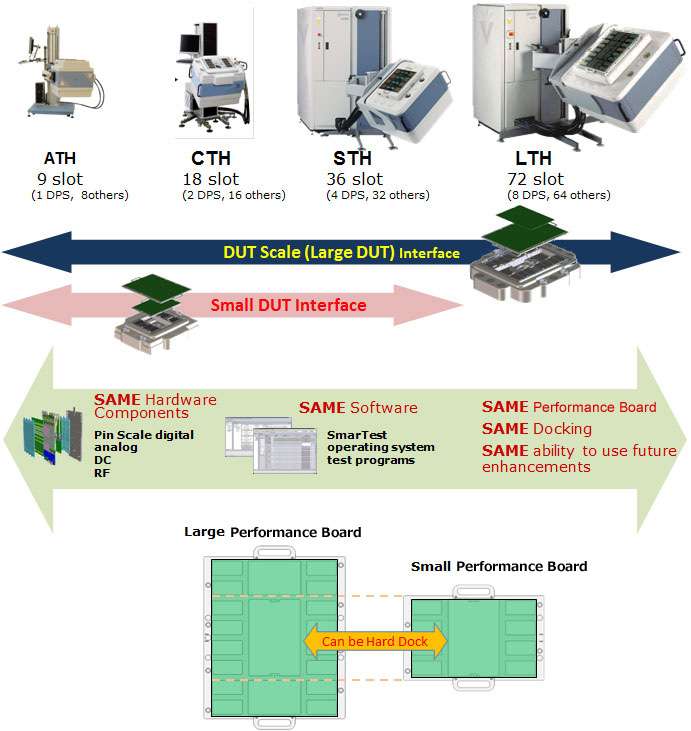
Picture: IC Tester (Source: Advantest)
19. Post-Silicon Validation
The samples that pass the tester are validated in a real environment. This is called post-silicon validation. In post-silicon validation, the IC is configured using a software tool on a computer and the test code is downloaded into the IC. The expected output is monitored, and all the features of the IC are verified. The illustration below depicts a post-validation setup:
Picture: Post-Silicon Validation in IC Design Flow(Source: Researchgate)
The Current Top 10 Semiconductor Companies by Market Share
In 1990, the U.S. accounted for 37% of global semiconductor fabrication capacity. By 2020 US share had fallen to 12%. In contrast, China had no capacity to produce semiconductors in 1990, but by 2020 it had nearly 13% of production. The Chinese share of global manufacturing is projected to reach 24% by 2030, which would make it the world leader. China aims to be the global leader in chip manufacturing by 2030 and is massively subsidizing its semiconductor industry in an attempt to get there.
The Current Biggest Semiconductor Companies
Before diving into the companies, it’s important to have context on their business. Also known as foundries, these semiconductor companies specialize in the fabrication or production of chips. “Fabless” chip makers—companies that design their chips and supply hardware but do not have fabrication plants—outsource chip production to foundries, primarily in Asia (Taiwan, China, South Korea and Japan).
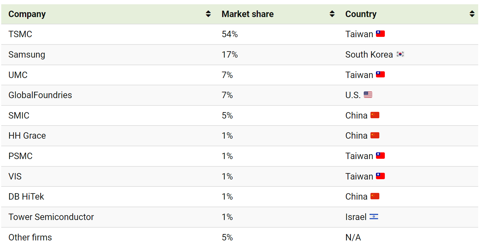
Taiwan, China, and South Korea combine for roughly 87% of the global foundry market. Here’s how it breaks down:
Top 5 Countries that Produces the Most Semiconductors:
1. Taiwan
2. South Korea
3. Japan
4. United States
5. China
Currently Which Country Fabricates the Most Semiconductor Chips?
1. Taiwan (63%)
The tiny East Asian country of Taiwan, whose diplomatic status is disputed by China, is the world’s undisputed leader in terms of raw semiconductor manufacturing. This is largely due to the work of a single company, Taiwan Semiconductor Manufacturing Co. (TSMC) which singlehandedly manufactures roughly 50% of the world’s semiconductors. Unlike semiconductor manufacturers such as Samsung or Intel, which produce semiconductors for use in their own products, TSMC manufactures semiconductors for many other companies, including Apple, AMD, Nvidia, Qualcomm, and more. This is known as the foundry model of business.
TSMC – TSMC operates four 12-inch wafer GIGAFAB® abs, four 8-inch wafer fabs, and one 6-inch wafer fab – all in Taiwan – as well as one 12-inch wafer fab at a wholly owned subsidiary, TSMC Nanjing Company Limited, and two 8-inch wafer fabs at wholly owned subsidiaries, TSMC Washington in the United States, and TSMC China Company Limited.
ASE Technology – ASE is the world’s leading provider of independent semiconductor manufacturing services in assembly and test.
UMC – UMC is best known for its semiconductor foundry business, manufacturing integrated circuits wafers for fabless semiconductor companies. In this role, UMC is ranked behind competitor TSMC. It has four 300 mm fabs, one in Taiwan, one in Singapore, one in China, and one in Japan.
2. South Korea (17%)
South Korea’s multinational Samsung Electronics corporation is one of the world’s largest technology companies in terms of revenue as well as one of the largest single semiconductor-producing companies in the world. Samsung functions as both an Integrated Devices Manufacturer (IDM), making semiconductors for use in its own products, and also as a foundry, producing semiconductors for other companies. Semiconductors produced by Samsung and other companies (such as SK Hynix) in the country’s 70+ fabrication plants are South Korea’s largest export, and comprised 15% of the country’s total exports in 2021.
Samsung – From south of Seoul to north of Austin, Samsung foundry superhighway builds and delivers the chips to make the world-class devices with almost two decades of reliable capacity and best-in-class cycle times.
SK hynix – SK hynix is the world’s second-largest maker of memory chips and a leading supplier of semiconductors. SK hynix produces dynamic random access memory (DRAM) chips, flash memory chips (NAND), and CMOS image sensors (CIS) for a wide range of distinguished global customers
3. Japan (13%)
One of the world’s most technologically advanced countries, the island nation of Japan is home to more than 100 semiconductor fabrication plants, most of which are owned by Japanese, American, or Taiwanese firms. As in other leading semiconductor manufacturing nations, the Japanese government is working to expand the country’s semiconductor manufacturing capabilities.
Renesas – In May 2022 Renesas announced the re-opening of its “Kofu” Fab which will utilize the 300mm geometry for the fabrication of power semiconductors. The facility is scheduled to be online in 2024.
Denso – Japanese automotive supplier Denso, opens new fab will invest about 500 billion yen ($3.3 billion) in semiconductors by 2030 as aims to triple the scale of its chips business by 2035 from current levels.
4. United States (7%)
The United States possessed approximately 12% of the world’s global chip manufacturing capacity as of 2021. This is a notably lower percentage of global capacity than the US enjoyed just a few decades previously (37% in 1990, for instance), before countries such as Taiwan and China ramped up their semiconductor production capabilities. Despite this decline, the semiconductor industry remains quite lucrative in the US. According to the Semiconductor Industry Association (SIA), semiconductors exports added $62 billion (USD) to the US economy in 2021, more than any product other than refined oil, aircraft, crude oil, and natural gas. Many of these imported chips return to the US in the form of finished consumer electronics.
Although the US held just 12% of the world’s total semiconductor manufacturing capacity in 2021, US-based companies held approximately 46.3 percent of the total semiconductor market share. This seeming discrepancy can be explained by both the dollar value of imported US semiconductors, outlined above, and the fact that many US-based companies own and operate semiconductor fabrication plants in other countries, such as Japan. In such cases, the manufacturing capacity is added to that country’s capacity rather than the capacity of the US, but the profits typically count as part of the US economy.
The COVID-19 pandemic caused a severe slowdown in the manufacture of semiconductors, as well as in the transport of both raw materials and finished semiconductors., triggering a worldwide shortage. In light of this complication, the US government is working to actively expand the country’s domestic semiconductor manufacturing capabilities.
Intel – Intel has 15 wafer fabs in production worldwide at 10 locations. Approximately half of our workforce handles production or production services.
Texas Instruments – LFAB2 will complement TI’s existing 300-mm wafer fabs, which include LFAB1 (Lehi, Utah), DMOS6 (Dallas), and RFAB1 and RFAB2 (both in Richardson, Texas). TI is also building four new 300-mm wafer fabs in Sherman, Texas (SM1, SM2, SM3 and SM4), with production from the first fab as early as 2025.
Micron – It’s current leading-edge chips are made in Japan and Taiwan, but Micron is aiming to bring advanced memory production to the U.S. starting in 2026 with a new $15 billion chip fabrication plant in Boise, Idaho. Micron celebrated its 45th anniversary in October by pouring the first cement at the new fab.
Nvidia – Nvidia does not manufacture its own chips. Instead, it outsources chip manufacturing to Taiwan Semiconductor Manufacturing Company (TSMC).
With lithography at the limits of physics, NVIDIA’s introduction of cuLitho and collaboration with our partners TSMC, ASML and Synopsys allows fabs to increase throughput, reduce their carbon footprint and set the foundation for 2nm and beyond.
5. China (7%)
One of the world’s primary manufacturing hubs, China is another country in the process of expanding its semiconductor manufacturing capacity. China is the world’s largest market for semiconductors, thanks in part to its massive manufacturing sector. Nonetheless, the Chinese government has set out to expand the country’s manufacturing capabilities to the point that China becomes self-reliant, producing the required amount of semiconductors domestically, with no need for imports. China is expected to produce up to 25% of the world’s semiconductors by the year 2030.
SMIC – Chinese pure-play foundry Semiconductor Manufacturing International (SMIC) is expected to open its largest-ever 12-inch (300mm) wafer manufacturing base in Lingang, Shanghai as early as the first quarter of 2024, according to industry sources.
Huawei – The Semiconductor Industry Association reportedly informed its members that Huawei has acquired two existing plants and is building three more. It has also received some $30 billion in government subsidies to help.
6. Europe & Middle East (6%)
STMicroelectronics – ST’s principal wafer fabs are located in Agrate Brianza and Catania (Italy), Crolles, Rousset, and Tours (France), and in Singapore.
Infineon – Infineon Technologies AG is Germany’s largest semiconductor manufacturer. The company was spun-off from Siemens AG in 1999. Infineon Technologies broke ground on May 2 2023 on its new 300-mm fab in Dresden, Germany for the construction of the €5 billion semiconductor plant.
NXP – NXP owns and operates four wafer fabrication facilities in the US, two of which are in Austin, Texas and two more in Chandler, Arizona. The representative products of these fabs include microcontrollers (MCUs) and microprocessors (MPUs), power management devices, RF transceivers, amplifiers and sensors.
7. South East Asia (4%)

Semiconductor manufacturing investments in the next 10 years in USA
The Semiconductor Industry Association (SIA) pointed out in a report that over 40 new semiconductor ecosystem projects have been announced across the U.S. since May 2020. We’re talking new fabs, expansions of existing sites, and also facilities that supply and produce materials and equipment for the semiconductor industry.
Count it all up and these projects are valued at nearly USD 200 billion in private investments, announced across 16 states. All of this means that about 40,000 new high-quality jobs are being created in the semiconductor ecosystem as part of the new projects.
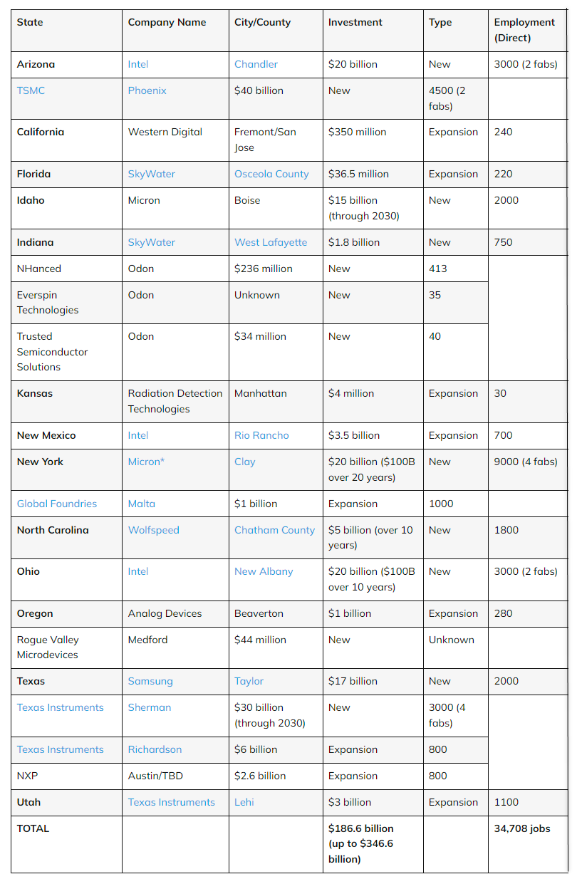
Source : globalsmt.net
Note: Micron announced total investments of up to USD 100 billion over a time frame beyond 10 years, however, this table only reflects investments made over the next decade.
Summary of IC Design Flow
ICs are of various types, and each IC type has certain characteristics: programmable or non-programmable, with or without a processor, high or low speed, compact or bulky. The process of designing, manufacturing, and testing an IC is complex and exhaustive. The main contributors are the design and verification teams, IP vendors, and IC manufacturers. Advanced EDA tools play a vital role in reducing the time and effort associated with the IC design cycle.
Glossary
| English Names for Flowers | In Kannada | In Kannada Font | In Tulu |
|---|---|---|---|
| Rose | Gulabi | ಗುಲಾಬಿ | Gulabi |
| Jasmine | Mallige | ಮಲ್ಲಿಗೆ | Mallige |
| Arabian Jasmine | Duṇḍu Mallige | ದುಂಡು ಮಲ್ಲಿಗೆ | Dundu Mallige |
| Coral Jasmine | Paarijaatha | ಪಾರಿಜಾತ | Paarijaatha |
| Crape Jasmine | Nandi Battalu | ನಂದಿಬಟ್ಟಲು | |
| Double Flowering Crape Jasmine | Nandi Battalu | ನಂದಿಬಟ್ಟಲು | Manjatti Poo |
| Cypress | Kaamalathe or Kempu Mallige | ಕಾಮಲತೆ or ಕೆಂಪು ಮಲ್ಲಿಗೆ | Jaaji |
| Four O’ Clock Flower | Sanje Mallige | ಸಂಜೆ ಮಲ್ಲಿಗೆ | Bayya Mallige |
| Chrysunthemum | Sevanthige | ಸೇವಂತಿಗೆ | Sevanthige |
| Dandelion | Kaadu Sevanthige | ಕಾಡುಸೇವಂತಿಗೆ | Kaad Sevanthige |
| Plumeria | Deva Kanagile | ದೇವ ಕಣಗಿಲೆ | |
| Cobra Saffron | Naaga Sampige | ನಾಗಸಂಪಿಗೆ or ನಾಗರ ಕೇಸರಿ | Naaga Sampige |
| Crossandra | Kanakambara | ಕನಕಾಂಬರ | Abbolige |
| Hibiscus | Dasavala | ದಾಸವಾಳ | Daasanaa |
| Marigold | Chendu Hoovu | ಚೆಂಡು ಹೂವು | Gonde Poo |
| Champak | Sampige | ಸಂಪಿಗೆ | Sampage |
| Golden Champak | Kenda Sampige | ಕೆಂಡ ಸಂಪಿಗೆ | Genda Sampage |
| Sunflower | Sooryakanthi | ಸೂರ್ಯಕಾಂತಿ | Sooryakanthi |
| Lotus | Thaavare | ತಾವರೆ, ಕಮಲ | Thaamare |
| Tube Rose | Sugnadharaja | ಸುಗಂಧರಾಜ | |
| Bluebellvine or Butterfly Pea | Shanka Pushpa | ಶಂಖಪುಷ್ಪ | Sanka Poo |
| Burflower | Kadamba Hoovu | ಕದಂಬ ಹೂವು | |
| Babool | Karijaali | ಕರಿಜಾಲಿ | |
| Crown Flower | Ekkada Hoovu | ಎಕ್ಕದ ಹೂವು | Ekkada Poo |
| Dahlia | Dere Hovvu | ಡೇರೆ ಹೂವು | |
| Dattura | Ummatti or Dattura | ಉಮ್ಮತ್ತಿ or ದತ್ತೂರ | |
| Lilly or Blue Water Lily or Water Lily | Naidile | ನೈದಿಲೆ ಹೂವು | |
| Fire Lilly | Agni Shikhe | ಅಗ್ನಿಶಿಖೆ | |
| Leucas | Thumbe Hoovu | ತುಂಬೆ ಹೂವು | Thumbe Poo |
| Oleander | Kanagile | ಕಣಗಿಲೆ | |
| Indian Oleander | Karaveera Pushpa | ಕರವೀರ ಪುಷ್ಪ | Karaveera Poo |
| Yellow Oleander | Kaadu Kanagile | ಕಾಡು ಕಣಗಿಲೆ | |
| Peacock Flower | Kenjige | ಕೆಂಜಿಗೆ | Kenjige |
| Periwinkle | Nithya Pushpa | ನಿತ್ಯಪುಷ್ಪ or ಸದಾ ಪುಷ್ಪ or ಬಟ್ಟಲು ಹೂವು | Nithya Poo |
| Queen of the Night | Brahma Kamala | ಬ್ರಹ್ಮಕಮಲ | Brahma Thaamare |
| Jungle Flame | Kiskara or Kepula Hoovu | ಕೇಪುಳ ಹೂವು | Kepula Poo |
| Egg Champak | Motte Sampige or Hima Sampige | ಮೊಟ್ಟೆ ಸಂಪಿಗೆ or ಹಿಮ ಸಂಪಿಗೆ | |
| White Garland-Lily or or White Ginger Lily | Sugandhi | ಸುಗಂಧಿ | Sugandhi |
| Skean | Suragi Hoovu | ಸುರಗಿ ಹೂವು | Surgi Poo |
| Magnolia | Champa | ಚಂಪಾ | |
| Balsam | Karnakundala | ಕರ್ಣಕುಂಡಲ | |
| Bougainvillea | Kagadada Hoovu | ಕಾಗದದ ಹೂ | Kaakaji Poo |
| Tulip | Kannada Pushpa | ಕನ್ನಡ ಪುಷ್ಪ | |
| Red lotus | Kempu Kamala | ಕೆಂಪು ಕಮಲ | Kempu Thaamare |
| Orchid | Archid | ಆರ್ಕಿಡ್ | |
| Primrose | Basanthi Gulabi | ಬಸಂತಿ ಗುಲಾಬಿ | |
| Poppy Flower | Khaskhas | ಖಸಖಸ್ | |
| Daisy | Daisy | ಡೈಸಿ | |
| Daffodils | Daffodils | ಡ್ಯಾಫೋಡಿಲ್ | |
| Indian Tulip | Adavi Bende Mara | ಅಡವಿಬೆಂಡೆ ಮರ | |
| Anemone | Hoogalige | ಹೂಗಳಿಗೆ | |
| Blood Lily | Raktha Naidile | ರಕ್ತ ನೈದಿಲೆ | |
| Globe Amaranth | Bili Rudrakshi | ಬಿಳಿರುದ್ರಾಕ್ಷಿ | |
| Lavender | Lavender | ಲ್ಯಾವೆಂಡರ್ | |
| Aloe Vera Flower | Ghruthakumari | ಘೃತಕುಮಾರಿ | |
| Delonix Regia | Gulmohar | ಗುಲ್ಮೊಹರ್ | |
| Pandanus | Kevada | ಕೇವಡಾ | |
| Mexican Tuberose | Rajanigandha | ರಜನೀಗಂಧಾ | |
| Mexican Prickly Poppy | Sathyanaashi | ಸತ್ಯನಾಶಿ | |
| Canna Lily | Sarvajna | ಸರ್ವಜ್ಞ | |
| Blue Morning Glory | Praatha Shree | ಪ್ರಾತಃ ಶ್ರೀ | |
| Butea Monosperma | Muttuga | ಬ್ರಹ್ಮವೃಕ್ಷ or ಮುತ್ತುಗ | |
| Common Lantana | Kaadujola | ಕಾಡುಜೋಳ or ಲಂಟವಾಣಿ | |
| Ashok Flower | Sitha Ashoka | ಸೀತಾ ಅಶೋಕ | |
| Pagoda Flower | Ratha Pushpa | ರಥ ಪುಷ್ಪ | Ratha Poo |
| Peackcok Flower | Rathna Gandhi or Meese Hoovu | Meese Poo | |
| Kewda, Fragrant Screw Pandanus odorife | Kedage | ಕೇದಗೆ | Kedage |
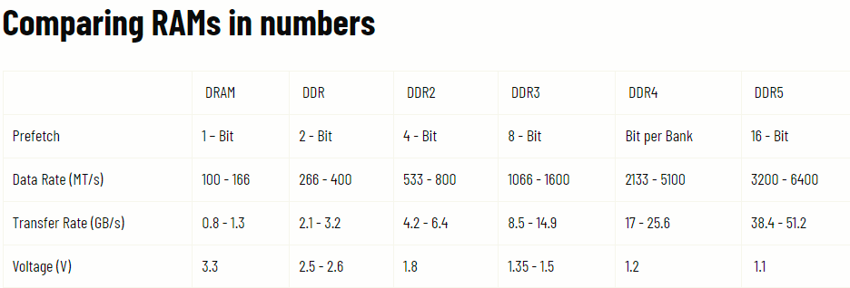
DDR and SRAM
- SDRAM was developed in 1988 in response to increased speeds of other computer components. The “synchronous” in its name is a clue — SDRAM modules are designed to automatically synchronize with the timing of the central processing unit (CPU).
- DDR – Short for Double Data Rate Was introduced in 2000 as the next generation following SDRAM. DDR transfers data to the processor on both the downbeat and upbeat of the clock signal, so twice per cycle. Using both beats to transfer data makes DDR memory significantly faster than SDR memory, which uses only one edge of the clock signal to transfer data.
- DDR2 – Was introduced in 2003 and operates twice as fast as DDR due to an improved bus signal. DDR2 uses the same internal clock speed as DDR, however, the transfer rates are faster due to the enhanced input/output bus signal. DDR2 has a 4-bit prefetch, which is twice that of DDR. DDR2 can also reach data rates of 533 to 800MT/s.
- DDR3 – In 2007 DDR3 technology was introduced with not only 2x the bandwidth and transfer rates of DDR2, but a significant reduction in power consumption – roughly 40% compared to DDR2.
- DDR4 – Seven years after the release of DDR3, DDR4 became available. The DDR4 has lower operating voltage with 1.2 V, and has higher transfer rates than previous generations, processing four data rates per cycle. This means DDR4 consumes less power and is faster and more efficient than DDR3.
- DDR5 – Was introduced in 2021, and is the most recent generation of memory technology, marking a revolutionary jump in architecture. It’s arguably the biggest jump in memory technology we’ve seen since SDRAM. DDR5 memory standard is a denser memory stick and equates to more memory capacity in your system. In comparison, the DDR4 stopped at 16-gigabit memory chips, but DDR5 offers up to 64-gigabit memory chips. Crucial DDR5 memory will operate at 4800MT/s at launch, 1.5x the maximum standard DDR4 speed.
DDR Comparison
USB
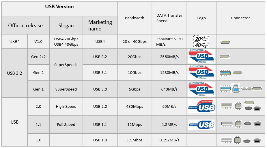
The Universal Serial Bus (USB) has quickly become an expected technology included in any new tech hardware. From smartphone chargers to flash drives and printer to computer connections.
But what is the difference between the two most common USB versions, USB 2.0, USB 3.0 and USB 4.0?. Here is the details:
All USB 3.2 Gen 2×2 products use the Type-C connector, but not all USB-C ports are USB 3.2 Gen 2×2. A USB-C port can be either 20Gbps USB 3.2 Gen 2×2 or 10Gbps USB 3.2 Gen 2. A USB Type-A port can be 10Gbps USB 3.2 Gen 2, 5Gbps 3.2 Gen 1 or even USB 2.0
USB Version Table







Great article to know the basics of ic design and testing … !!! A must read article for all engineers who are interested in the VLSI technology