

Simplest Guide to RTL Design, Verification and Synthesis – VLSI Verification Flow
Abstract
This article provides an overview of Register Transfer Level (RTL) Design, Verification and Synthesis Flow. In simple term, this is called VLSI/ASIC Verification Flow or the Frontend Design of the the VLSI Flow. It describes the fundamentals of RTL design and the process of RTL design. The article will also discuss RTL synthesis, RTL for synchronous and asynchronous design, RTL simulation, RTL in FPGA and ASIC and RTL design tools. The main objective of this article is also to explain Synthesis Flow and post-synthesis netlist quality checks. In ASIC flow, synthesis is the part of the Frontend Design, while the Backend Design takes the synthesized netlist as an input. So, the synthesized netlist should meet all netlist quality checks to reduce multiple iterations, which reduces the turnaround time and efforts.
We will see the overview of various checks that are performed at the synthesis stage of the ASIC Flow in this article. After reading this article, you will be able to answer the following questions:
- What RTL is synthesis?
- Why do we need RTL design, verification and synthesis?
- What are the input and output of the RTL design and synthesis?
- What is verification, EDA tools used for verification flow and what is synthesis flow and also the EDA tools used for synthesis flow.. etc?
- What are the checks performed to ensure the netlist or gate level netlist quality during synthesis?
Introduction
What is RTL?
Register-Transfer Level (RTL) design is a critical aspect of digital circuit design. It is a design abstraction representing how data flows between hardware registers (For example 8-bit register) and the operations performed on that data. RTL design approach is used in creating digital systems where the flow of data between registers, and the operations on that data, are important for the system’s functionality.
As digital circuits become more complex, and demand for more efficient systems increases, RTL design has become an essential skill for design engineers alike. It provides a level of abstraction that enables efficient design and verification of complex digital systems. The importance of RTL design is further underscored by its role in the design of microprocessors, digital signal processors, and other complex integrated circuits.
RTL design provides an abstraction that makes it possible to design and verify systems that contain millions of transistors. It provides a manageable way to design complex digital systems and is a critical step in transforming a high-level system description into a
What is Synthesis?
Synthesis transforms the RTL code of design modules into a gate-level netlist. This stage performs logic, area, power optimization, and scan insertion (DFT insertion with ATPG). Various commercial EDA tools are available, which can be used to do synthesis such as Synopsys Design Compiler/Fusion Compiler or Cadence Genus. or Synopsys Precision RTL(entry-level FPGA synthesis ) or Oasys RTL (For IP Qualification)
The Basics of RTL Design
Register-Transfer Level (RTL) design is a methodology used for designing digital circuits. The term “register-transfer” refers to the level of abstraction at which the design is considered. At this level, the design is described in terms of the flow of data between registers, and the logic operations that take place on that data.
In RTL design, the designer specifies the data operations to be performed, and the flow of data between registers. The designer does not need to specify how these operations are to be implemented in the hardware. This level of abstraction allows the designer to focus on the high-level function of the system, without getting stuck in the details of the implementation.
RTL design is typically done using a hardware description language (HDL) such as VHDL , Verilog or SystemVerilog. These languages provide constructs that allow the designer to describe the system in terms of registers, operations, and data flows. The use of an HDL allows the designer to describe the system in a way that is independent of the specific hardware that will be used to implement the system.
Understanding Registers
In RTL design, a register is a hardware element that can store a fixed amount of data. The data stored in a register can be used as input to a logic operation, and the result of the operation can be stored back in the register. Registers are the basic building blocks of digital systems, and the flow of data between registers is a key aspect of the system’s function.
Registers in RTL design are typically binary, meaning they store data in the form of binary digits, or bits. The number of bits a register can store is referred to as the width of the register. For example, a register that can store 8 bits of data is called an 8-bit register.
The data stored in a register is often referred to as the state of the register. The state of a register can change over time as new data is stored in the register. The sequence of states that a register goes through over time is a key aspect of the behavior of the digital system.
In RTL design, registers are used to hold the inputs, outputs, and intermediate results of the logic operations performed. The designer specifies the sequence of operations to be performed and the flow of data between registers to implement the desired function of the system.
Understanding Operations
In RTL design, operations are the logic functions that manipulate and process the data stored in registers. These operations are the fundamental building blocks of digital systems and are responsible for implementing the desired functionality of the system. Operations in RTL design can be broadly categorized into two types: arithmetic operations and logical operations.
Arithmetic operations are used to perform mathematical calculations on the data stored in registers. Some common arithmetic operations include addition, subtraction, multiplication, and division. These operations are typically implemented using dedicated hardware elements, such as adders, subtractors, multipliers, and dividers. In RTL design, arithmetic operations are specified using the appropriate constructs in the hardware description language (HDL), such as VHDL or Verilog.
For example, in VHDL, an addition operation can be specified as follows:
sum <= a + b;
In this example, a and b are input registers, and sum is the output register that stores the result of the addition operation.
Logical operations are used to perform bitwise manipulation of the data stored in registers. Some common logical operations include AND, OR, NOT, XOR, and shift operations. These operations are implemented using basic logic gates, such as AND gates, OR gates, and inverters. In RTL design, logical operations are specified using the appropriate constructs in the HDL.
For example, in Verilog, an AND operation can be specified as follows:
assign result = a & b;
In this example, a and b are input registers, and result is the output register that stores the result of the AND operation.
In RTL design, operations are used to implement the desired functionality of the system by processing the data stored in registers. The designer specifies the sequence of operations to be performed and the flow of data between registers to achieve the desired system behavior. The designer can efficiently design and verify complex digital systems by focusing on the operations and data flow at the RTL level.
Synchronous and Asynchronous Logic
At the heart of digital circuit design, two fundamental approaches orchestrate data flow: synchronous and asynchronous logic. Within RTL design, they each play distinct roles, shaping how systems operate and interact. While synchronous logic relies on a global clock signal to guide operations, asynchronous logic empowers elements to move independently, guided by local signals.
Any digital circuit whether combinational or sequential, can be designed using RTL. RTL logic can be implemented in a similar fashion to event-based or clock-based logic. The event-based reset logic in that code, which is independent of other events, allows the circuit to be reset, as shown in the figure below. The TL logic for asynchronous logic is shown in the figure:
async_reset process(clk, rst) is
begin
    if rst = '1' then ; asynchronized reset signal
       q <= '0' ;
    elsif rise_edge(clk) then
        q <= d ;
    end if ;
end process async_reset;
Additionally, events in synchronous logic depend on the synchronization of the clock as depicted below.
sync_reset process(clk) is
begin
    if rise_edge(clk) then ; synchronized with the rising edge of the clock
       if rst = '1' then
          q <= '0' ; ; output status of 1 goes 0 if rest is 1 and with is synchronized with the rising edge of the clock
      else
          q <= d ;
      end if ;
    end if;
end process sync_reset;
In general, synchronous logic is the preferred choice for most digital systems due to its predictability and ease of design. However, asynchronous logic can offer advantages in specific applications where power consumption or performance is critical.
Note: Any circuit, from asynchronous to synchronous, may be designed using the RTL
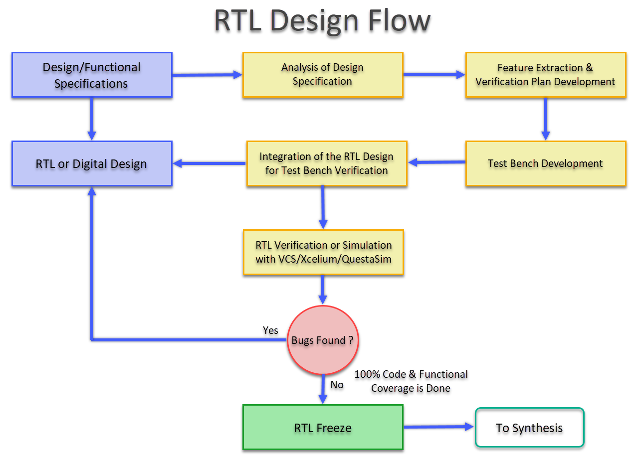
The RTL Design Process
The RTL design process is a series of steps that transform a high-level system description into a low-level implementation that can be fabricated onto a chip. This process, also known as front end involves several key stages, including high-level synthesis, RTL coding, and RTL verification.
The first stage of the RTL design process is high-level synthesis, where a high-level description of the system is transformed into an RTL description. This involves translating the system’s behavior, specified in a high-level language such as C or C++, into an equivalent RTL description in a hardware description language (HDL) like VHDL or Verilog.
The next stage is RTL coding, where the RTL description is further refined and optimized. This involves writing the RTL code that describes the data flow and operations of the system, and optimizing this code to meet the design requirements.
The final stage is RTL verification, where the correctness of the RTL design is checked. This involves simulating the RTL design to ensure it behaves as expected, and formally verifying the design to prove its correctness.
Let’s take a closer look at each of these stages.
High-Level Synthesis (HLS)
High-level synthesis (HLS) is the process of transforming a high-level system description into an equivalent RTL description. This involves translating the system’s behavior, specified in a high-level language such as C or C++, into an equivalent RTL description in a hardware description language (HDL) like VHDL , Verilog or SystemVerilog.
HLS is a critical step in the RTL design process as it allows designers to describe the system’s behavior in a high-level language, which is easier to understand and write than low-level HDL code. This not only speeds up the design process but also reduces the chance of errors.
During HLS, the high-level system description is analyzed, and the data flow and operations of the system are extracted. These are then mapped onto an RTL description, which describes the system in terms of registers, operations, and data flows.
For example, consider a high-level description of a system that performs a simple arithmetic operation, such as adding two numbers. The HLS process would analyze this description, extract the addition operation and the data flow between the input and output, and map these onto an RTL description that specifies the addition operation and the flow of data between registers.
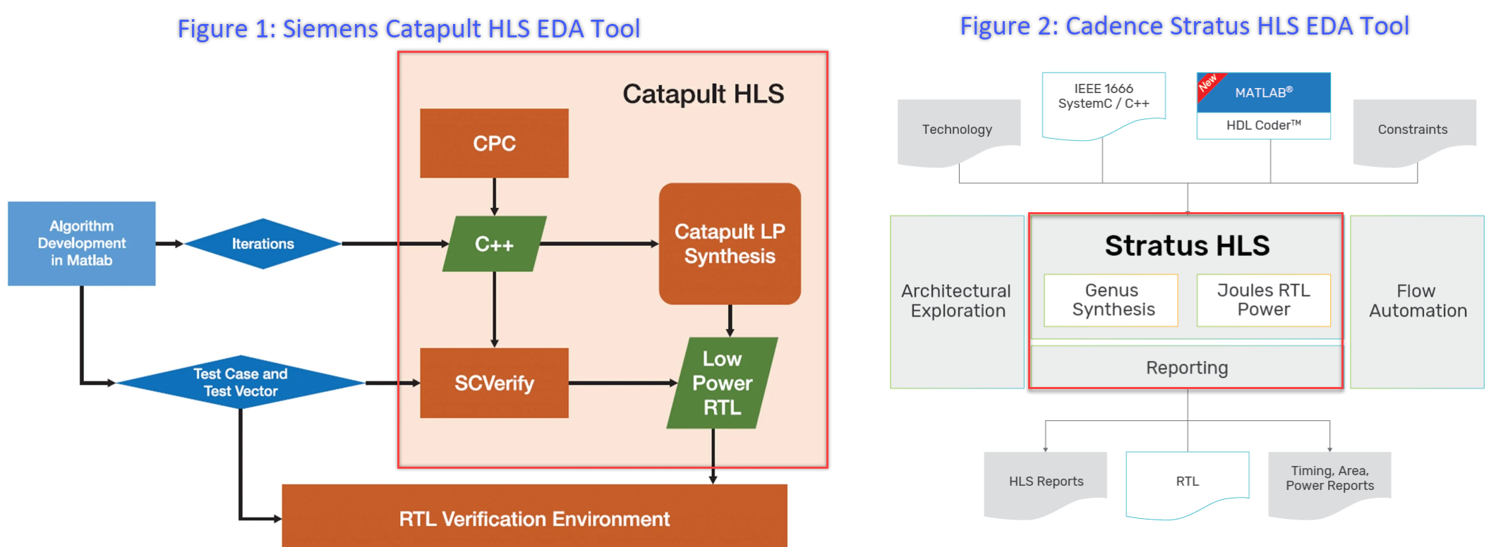
HLS tools, such as Cadence Stratus or Siemens’ Catapult, automate this process, allowing designers to quickly and accurately generate RTL descriptions from high-level system descriptions. These tools also provide optimization features that can improve the performance, power, and area of the resulting RTL design.
RTL Coding
RTL coding is the process of writing the RTL description of a digital system using a hardware description language (HDL) such as VHDL or Verilog. This stage of the RTL design process involves specifying the data flow and operations of the system in terms of registers, operations, and data flows. RTL coding is crucial for defining the system’s behavior and ensuring that it meets the design requirements.
During RTL coding, the designer writes the HDL code that describes the system’s registers, operations, and data flows. This code is typically organized into modules, which are reusable blocks of code that represent specific parts of the system. Modules can be instantiated multiple times within a design, allowing for efficient reuse of code and simplification of the overall design.
VHDL and Verilog are the two most widely used HDLs for RTL coding. Both languages provide constructs for describing registers, operations, and data flows, as well as control structures for specifying the sequence of operations.
VHDL (VHSIC Hardware Description Language) is a strongly typed, concurrent language that provides a high level of abstraction for describing digital systems. It supports a wide range of data types and constructs, making it suitable for describing complex systems. VHDL code is typically organized into entities and architectures, where entities define the interface of a module, and architectures define the behavior of the module. [5]
For example, a simple VHDL module that implements a 4-bit adder might look like this:
entity adder is
  port (
    a, b: in std_logic_vector(3 downto 0);
    sum: out std_logic_vector(3 downto 0)
  );
end entity adder;

architecture behavior of adder is
begin
  sum <= a + b;
end architecture behavior;
Verilog is a weakly typed, concurrent language that provides a lower level of abstraction than VHDL. It is well-suited for describing digital systems at the gate, register-transfer, and behavioral levels. Verilog code is typically organized into modules, which define both the interface and behavior of a part of the system.
For example, a simple Verilog module that implements a 4-bit adder might look like this:
module adder (
  input [3:0] a, b,
  output [3:0] sum
);
  assign sum = a + b;
endmodule
During the RTL coding stage, the designer must ensure that the HDL code accurately describes the desired behavior of the system and meets the design requirements. This may involve optimizing the code for performance, power, and area, as well as ensuring that the code is modular and reusable. Once the RTL coding is complete, the design moves on to the RTL verification stage, where the correctness of the RTL description is checked.
RTL Verification
RTL verification is the final stage in the RTL design methodology, where the correctness of the RTL design is checked. This stage is crucial to ensure that the RTL description accurately represents the intended behavior of the digital system and meets the design requirements. There are two main methods used in RTL verification: simulation and formal verification.
Verification is crucial to ensure the design’s correctness, robustness, and reliability.
- Simulation is a dynamic verification method where the RTL design is tested by applying a set of input vectors and observing the resulting output vectors. The input vectors are typically derived from the system’s specifications and are designed to exercise all the functional aspects of the system. The output vectors are then compared with the expected results to check the correctness of the design.
Digital Simulation tools, such as VCS (VLSI Designer’s Choice) from Synopsys or ModelSim from Siemens or Xcelium from Cadence, are used to perform RTL simulation or verifications. These tools execute the RTL code and provide a waveform view of the signals in the design, allowing the designer to visually inspect the behavior of the system.
For example, in a simulation of a 4-bit adder, the input vectors might be pairs of 4-bit numbers, and the expected output vectors would be the sums of these numbers. The simulation tool would apply these input vectors to the adder, observe the resulting output vectors, and compare them with the expected results to verify the correctness of the adder.
2. Formal Verification is a static design verification method that mathematically proves the correctness of the RTL design. This involves expressing the intended behavior of the system as a set of formal properties, and then using a formal verification tool to prove that these properties hold for the RTL design.
Formal verification tools, such as Cadence’s JasperFormal/JasperGold or Synopsys’ VC Formal/SpyGlass, or Siemens LedaRTL/Questa-Formal-Verification use mathematical algorithms to exhaustively explore the state space of the design and prove the correctness of the formal properties. This provides a higher level of assurance of the design’s correctness than simulation, as it can prove the correctness of the design for all possible input vectors, not just a subset. UVM is also a standardized framework for creating reusable and scalable testbenches, streamlining verification processes in RTL design.
For example, in a formal verification of a 4-bit adder, the formal properties might specify that for any pair of 4-bit numbers, the output of the adder is the sum of these numbers. The formal verification tool would then mathematically prove that this property holds for the RTL description of the adder.
RTL verification is a critical stage in the RTL design process, as it ensures that the RTL description accurately represents the intended behavior of the system and meets the design requirements. By using simulation and formal verification methods, designers can confidently verify the correctness of their RTL designs and proceed to the next stages of the design process.
Advanced Concepts in RTL Design
Advanced concepts in RTL design involve techniques and methodologies that go beyond the basic RTL design process. These include RTL partitioning, pipelining, and clock domain crossing, among others. These advanced concepts are used to manage the complexity of large designs, optimize the performance, power, and area of the design, and handle special design requirements.
RTL Partitioning
RTL partitioning is a technique used to manage the complexity of large RTL designs. It involves dividing the design into smaller, more manageable parts, or partitions, each of which can be designed and verified independently. This not only simplifies the design process but also allows for parallelism, where different partitions can be designed and verified by different designers or teams at the same time.
Partitioning can be done in several ways, depending on the requirements of the design. One common method is functional partitioning, where the design is divided based on its functional blocks. For example, in a microprocessor design, the processor core, memory, and input/output (I/O) interfaces might be separate partitions.
Another method is hierarchical partitioning, where the design is divided into a hierarchy of partitions. This is often used in complex designs that consist of several layers of hierarchy, with each layer representing a different level of abstraction.
Partitioning can also be done based on the physical characteristics of the design, such as low-power domains or clock domains. This is known as physical partitioning and is used for power estimation and timing analysis of design.
RTL partitioning is a powerful technique for managing the complexity of large designs. By dividing the design into smaller, more manageable parts, designers can focus on the details of each part without being overwhelmed by the complexity of the whole design. This not only simplifies the design process but also improves the quality of the design, as each part can be thoroughly designed and verified.
RTL Optimization
RTL optimization is a critical step in the RTL design process that aims to improve the performance, power, and area (PPA) of the design. [6] This involves refining the RTL description to make it more efficient and effective in meeting the design requirements.
- Performance optimization involves improving the speed of the design. This can be achieved by techniques such as pipelining, where the design is divided into stages that can be executed in parallel, and parallelism, where multiple operations are performed simultaneously. For example, in a processor design, instruction fetching, decoding, execution, and write-back can be pipelined to improve the processor’s instruction throughput.
2. Power optimization involves reducing the power consumption of the design. This can be achieved by techniques such as clock gating, where the clock signal is disabled for parts of the design that are not in use, and power gating, where the power supply is cut off to parts of the design that are not in use. For example, in a mobile device design, power gating can be used to turn off the GPS module when it is not in use to save power.
3. Area optimization involves reducing the size of the design. This can be achieved by techniques such as resource sharing, where multiple parts of the design share the same resources, and constant propagation, where constants are propagated through the design to simplify operations. For example, in a digital signal processing (DSP) design, multiple filters can share the same multiplier to save area.
RTL optimization is performed using RTL synthesis tools, such as Synopsys’ Design Compiler or Cadence’s Genus. These tools analyze the RTL description and apply various optimization techniques to improve the PPA of the design. The designer can guide the optimization process by setting constraints on the performance, power, and area of the design, and the synthesis tool will try to meet these constraints while optimizing the design.
RTL optimization is a complex and challenging task that requires a deep understanding of the design and the optimization techniques. However, it is a crucial step in the RTL design process, as it can significantly improve the PPA of the design and make it more competitive in the market.
Challenges and Solutions in RTL Design
RTL design, while a powerful methodology for digital system design, presents several challenges. These include handling design complexity, managing power consumption, and ensuring design correctness. However, various solutions have been developed to address these challenges, including RTL partitioning, power optimization techniques, and formal verification methodology.
Handling Design Complexity
One of the main challenges in RTL design is managing the complexity of large designs. As the size and complexity of digital systems continue to grow, the task of designing and verifying these systems at the RTL level becomes increasingly difficult. This complexity can lead to longer design times, increased risk of design errors, and difficulty in meeting performance, power, and area requirements.
- RTL Partitioning is a key technique for handling design complexity. By dividing the design into smaller, more manageable parts, designers can focus on the details of each part without being overwhelmed by the complexity of the whole design. This not only simplifies the design process but also improves the quality of the design, as each part can be thoroughly designed and verified.
Another approach to managing design complexity is the use of high-level synthesis (HLS) tools. These tools allow designers to describe the design at a higher level of abstraction using a high-level programming language, such as C or C++. The HLS tool then automatically generates the RTL description from the high-level description. This not only reduces the complexity of the design process but also allows designers to leverage their software programming skills.
2. Design Reuse is another effective strategy for managing design complexity. By reusing proven design blocks, or IP cores, designers can reduce the amount of new RTL code that needs to be written and verified. This not only saves design time but also reduces the risk of design errors.
By using techniques such as RTL partitioning, high-level synthesis, and design reuse, designers can effectively manage the complexity of large designs and produce high-quality, efficient digital systems.
Ensuring Design Correctness
Ensuring design correctness is another significant challenge in RTL design. Given the complexity of modern digital systems, verifying that the RTL description accurately represents the intended behavior of the system is a non-trivial task. Errors in the RTL description can lead to functional errors in the final system, which can be costly to fix if not detected early in the design process.
- Simulation is a widely used method for checking design correctness. By applying a set of input vectors to the RTL design and observing the resulting output vectors, designers can check whether the design behaves as expected. However, due to the exponential growth of the state space with the size of the design, it is impossible to simulate all possible input vectors for large designs. Therefore, creating a comprehensive set of test vectors that can effectively exercise all functional aspects of the design is a challenging task.
2. Formal Verification offers a solution to this challenge. By expressing the intended behavior of the system as a set of formal properties, and using a formal verification tool to mathematically prove that these properties hold for the RTL design, designers can ensure the correctness of the design for all possible input vectors. However, writing the formal properties and interpreting the results of the formal verification tool requires a high level of expertise.
Another approach to ensuring design correctness is the use of assertion-based verification (ABV). In ABV, designers write assertions, which are statements of intended behavior, in the RTL code. [7] These assertions are then checked during simulation or formal verification. If an assertion fails, it indicates a discrepancy between the intended and actual behavior of the design.
3. Linting is another technique used to ensure design correctness. Linting tools perform static analysis of the RTL code to check for common coding errors, adherence to coding standards, and potential synthesis and timing issues. By catching these issues early in the design process, linting tools can help improve the quality of the RTL code and reduce the risk of design errors.
By using a combination of simulation, formal verification, assertion-based verification, and linting, designers can ensure that the RTL description accurately represents the intended behavior of the system and meets the design requirements.
Implementing RTL Design in a Real-World Scenario
A real-world example of implementing RTL design can be seen in the development of a digital signal processing (DSP) system for a wireless communication device. The DSP system is responsible for processing the digital signals received from the wireless interface, and performing operations such as filtering, modulation, and demodulation.
The first step in the RTL design process was to define the specifications of the DSP system. These specifications included the types of signals to be processed, the required processing operations, and the performance, power, and area requirements of the system.
Next, the RTL description of the DSP system was written using a hardware description language, such as VHDL, or Verilog or SystemVerilog. The RTL description defined the data paths and control logic of the DSP system, including the registers, arithmetic units, and control units.
The RTL description was then verified using simulation and formal verification methods. For simulation, a set of test vectors was created based on the system’s specifications, and these vectors were applied to the RTL design using a simulation tool. The output vectors were observed and compared with the expected results to check the correctness of the design.
For formal verification, a set of formal properties was written to express the intended behavior of the DSP system. A formal verification tool was used to mathematically prove that these properties hold for the RTL design.
After the RTL design was verified, it was optimized using an RTL synthesis tool. The tool analyzed the RTL description and applied various optimization techniques to improve the performance, power, and area of the design. The designer guided the optimization process by setting constraints on the performance, power, and area of the design.
Finally, the optimized RTL design was translated into a gate-level netlist using the synthesis tool. The netlist was then used for physical design, where the layout of the DSP system was created for fabrication. Testbench is used as a virtual environment to simulate and verify the functionality and timing of an RTL design before physical fabrication in VLSI.
This case study illustrates the application of RTL design in a real-world scenario. Despite the complexity of the DSP system, the RTL design process enabled the designers to effectively manage the design complexity, ensure the correctness of the design, and optimize the performance, power, and area of the system.

RTL Usage in FPGA/ASIC Design Flow
The advancement in the RTL languages RTL design flow is also part of the ASIC design flow. Instead of designing the ASIC from scratch, which also involves writing the libraries, the designer can write the functionalities of these circuit in RTL and generate the gate-level netlist, that further used to make the layout for the ASIC design. Figure 5 shows the design flow for ASIC and FPGA design. Both have the same initial design flow starting from the design specification and RTL. Either you want to do the RTL for FPGA and ASIC, the RTL design will remain the same. The difference starts after synthesizing FPGA does not require designer efforts to do floor planning and place and route instead done by the tool. ASIC designer needs to do the floor planning and route to optimize the design for better performance.

EDA Tools for RTL Design
The major players in the area of RTL tools are the following:
- Synopsys – Fusion Compiler (From RTL Design to Sign-off) including VCS
- Cadence ─ Genus (RTL Synthesis Tool)
- Siemens – Catapult (RTL Synthesis Tool)
- Xilinx/AMD ─ Vivado
- Intel/Altera ─ Quartus
Synthesis overview
Once the RTL of the design fulfills all criteria of RTL checks, then the next step is synthesis. Synthesis is the stage where the RTL code is converted into a gate-level netlist.
Synthesis is one of the important steps in chip designing flow as it allows us to visualize the design as it will appear after manufacturing. Here, designers review all reports and validate all required factors including timing, area, and power. Designers can make necessary changes (if required) before the creation process, which saves time, money, and effort.
The synthesis process can be divided into three stages:
- Translation
- Optimization
- Mapping

Figure – Steps in Synthesis
Input
- Timing library (.lib or .db)
- Physical Library (lef, Milkyway)
- SDC
- RTL
- DEF (For Physical aware Synthesis)
- TLU+(Synopsys), Qrc(cadence) file
- UPF
Output
- Netlist
- UPF
- SDC
- DEF
- Reports
Goal of Synthesis
- Logic optimization with good QoR
- Scan insertion (DFT)
- Netlist generation
- Logical equivalence check should be preserved between the RTL and netlist
Types of Synthesis
1. Logical Synthesis
Logical synthesis is a conventional synthesis, that processes the HDL (Verilog or VHDL) design and generates gate level netlist. During this process, the compiler optimizes the design based on predefined constraints.
2. Physical Aware Synthesis
Physical Aware synthesis requires additional floorplan DEF as an input. Floorplan DEF contains physical information like IO ports placements, macro placement information, blockages information and die area information. Additionally, we use RC co-efficient file as one of the inputs to compute a more accurate wire delay values compared to the WLM (Wire Load Model) method.
Advantages of Physical Aware synthesis:
- Better PPA (Power, Performance, Area).
- Better timing correlation with PNR.
- Better turnaround time (reduces the number of iterations).
Synthesis Flow
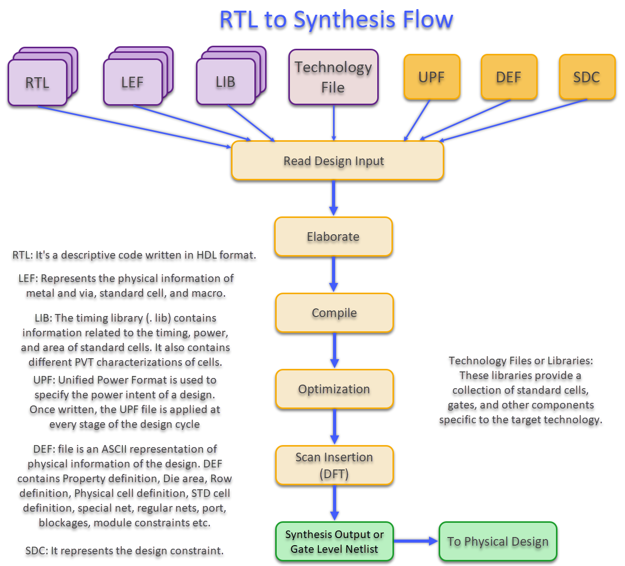
Figure – Synthesis Flow
Synthesis input
- LIB: The timing library (.lib) contains information related to the timing, power, and area of standard cells. It also contains different PVT characterizations of cells.
- LEF: Library Exchange Format (LEF) represents the physical information of metal and via, standard cell, and macro.
- RTL: It’s a descriptive code written in HDL format.
- SDC: Synopsys Design Constraints (SDC) format is used to specify the design intent, including timing, power and area constraints for a design. This format is used by different EDA tools to synthesize and analyze a design. SDC is based on the tool command language (Tcl).
- DEF: Design Exchange Format (DEF) file contains the placement information of macro, pre-placed cells, IO ports, block size, and blockages. Mainly used for the Physical Aware synthesis.
- UPF: Unified Power Format (UPF) was developed within Accellera. UPF file is required to describe the power intent of the design including the power domain, level shifter, isolation cell, and retention registers.
Elaboration
At this stage, it reads the RTL code, and this RTL code is converted into modules as per its logical hierarchy. Once it has all logical Boolean representation loaded, the tool maps logic with a technology-independent cell called the Gtech cell.
During elaboration, the tool checks whether the design is unique, if not, it stops the tool. Once the design becomes unique, the tool checks for unresolved references in the design. If it has linking issues, then an RTL correction is required, or you need to check if it is due to any missing libraries. After elaboration, it checks for timing loops in design. If you find any timing loop, you need to get RTL correction done by the designer.
Compile and Optimization
After elaboration, in the compilation stage, the tool maps the Gtech cell with the actual cell (specific technology dependent) from the library. Actual cell mapping is dependent on the design constraints or user-specific constraints. Apart from this, the tool removes the registers with constant propagation/unloaded which are not required in the design. If these removed cells are required, then you need to provide feedback to the designer to get the correct RTL.
After elaboration and compilation, the tool performs optimizations based on user constraints to meet timing, area, and power requirements.
DFT
The Design for Testability (DFT) stage performs the scan insertion in the optimized design. After this stage, the design should fulfill the scan criteria and achieve the desired scan coverage.
Outputs
A qualified netlist with scan insertion and good QoR in terms of timing, power, and area. Other outputs are updated DEF, UPF, and SDC.
- UPF: The output UPF is the updated version of the input UPF. At the synthesis stage, it performs logic optimization that introduces new power intents. So, we are generating UPF with this update after synthesis.
- DEF: While performing Physical Aware synthesis, we also generate the DEF file, which contains macro and standard cell placement information. This DEF is directly used in physical implementation that, avoids placement of the cell from scratch, hence, we can save run time.
- SDC: The output SDC is the updated version of the input SDC. At the synthesis stage, we use constraints provided by the designer. Additionally, we use certain local constraints to improve the overall QoR of design. Thus, the SDC with this update is generated after synthesis.
Netlist Quality Checks, Logic Equivalence Checks (LEC) & Timing Checks
Below are certain checks that, should be fulfilled post-synthesis to ensure netlist qualifications before it is delivered for physical implementation.
1. No Clocks:
In this check, we ensure that all the required clocks reach the sync points. Some major reasons for getting no clock violation in design are mentioned below:
- Clock definition missing: This is observed when clock creation is missing in the clock constraint file.
- RTL connectivity issue/Tie off: This type of no clock is observed when there is missing connectivity in between modules in the RTL or having direct tie-offs in the RTL.
Impact: Ideally, all the registers in the design should be clocked. If no clock issue is left in the design, then it will report unconstraint endpoints and can cause optimization issues on such paths.
Solution: To resolve the above-mentioned no clocks violation, we need to get the corrected RTL (from the designer) and clock constraints files with all the required clock definitions.
Command: check_timing -include {no_clock}
2. Unconstraint end-points:
This is due to the missing IO constraints, clock definitions, or due to some exceptions at the sequential cells or ports. Possible reasons are case constant, no arrival path, or false path.
Impact: If IO constraints are missing in the design, then the external launch time for the input path or the capture time for the output path will be missed. It can cause an incomplete timing check. If the path is expected to be false, it could lead to an incorrect timing check.
Solution: To resolve these problems, we need the correct constraint file (sdc), which defines all the required clocks used in the design, IO delays on all the required ports, verified false path, and case constants in design.
Command: check_timing -include {unconstrained_endpoints}
3. Timing:
In this check, the entire design is divided into timing paths. For each timing path, the delay is calculated and checks violation based on timing constraints (clock period, clock uncertainty, and setup time). The major reasons for having timing violations are- levels of logic, incorrect/missing constraints such as clock relations, clock exceptions, and incorrect uncertainty.
Impact: If a huge timing violation is reported at the synthesis, this violation will be difficult to fix at later stages (PNR/ECO), which also impacts the power and area.
Solution: The techniques used to resolve/reduce timing violations are user-defined path groups with appreciate weightage, by disabling selectively/entirely multibit banking in design, bound creation, using timing efforts high or incremental compilation. If we are performing Physical Aware synthesis, it is expected to have a good macro placement that improves timing violations.
Command: report_timing or report_qor
4. LEC:
This is one of the important checks that validate the correctness of the netlist concerning the RTL.
It is recommended to perform this check when there is an update in the RTL or netlist. Generally, in the synthesis LEC, a check is performed between the RTL vs synthesize netlist and synthesize netlist vs post scan netlist.
General issues due to which the LEC can fail are as follows:
- CSN Missing: The missing CSN (Connect Supply Net) can lead to LEC failure.
- Isolation cell mapping: When there is an issue with UPF constraint, then there could be a possibility of having different isolation cells, mapped in between the RTL and synthesize netlist, that may cause LEC failure.
- Undriven Nets: If we have undriven nets in the RTL, the synthesize tool will tie off these nets causing LEC failure. This can be resolved by getting the RTL fixed or if the undriven is expected, then you need to use undriven constraints to pass the LEC.
Constraint used (formality): set_constants <net_name> <0/1>
Impact: If the LEC is not clean then the equivalence is not maintained between the RTL and netlist which can lead to functionality failure.
EDA Tool: Formality from Synopsys, conformal from Cadence
5. Timing loop:
In the RTL, if in between combo logic, the output is again feed to the same input of combo logic that forms a logical loop, this loop is called the timing loop. We can get the timing loops due to RTL connectivity issues in design that, which can lead to meta-stable data, thus, we should avoid timing loops while netlist generation.
Impact: The path with timing loops will not have endpoints. If such loops are not broken then the path will not be correctly timed.
Solution: If we are getting timing loops that are expected to have then in such case, we need to use the constraint to break such timing loops. If such timing loops are not expected in design, then we need to get the updated RTL.
Command: check_timing -include {loops}
6. Empty module:
If the RTL module definitions don’t have any logical content such as wire, inputs, or outputs, then such modules are called empty modules. This check is performed before compilation.
By default, empty modules are removed during synthesis. If we want to preserve this empty module, we need to apply constraint (set_dont_touch) on that module before compilation.
Command: check_design
7. Removed Flop:
If the register is removed during compilation and optimization, then such flop is reported as removed flops. If the register is either unloaded or constant, then by default during compilation such flip flop is removed from the design.
If such flip flops are expected in design, then we need to use certain constraints to preserve this.
Command:
report_unloaded_registers
report_constant_registers
8. Floating pins and multidriven pins:
In the design there might be a possibility that a few of the pins are not connected to any element present in the design. Such pins are known as floating pins. While performing optimization, such floating pins cells might get optimized due to which there could be a breakdown in logic.
Multidriven nets are detected when there is more than one input connected to the same net from different modules. This is not accepted in design and you need to fix this issue. It requires RTL correction to resolve this issue.
9. Latches:
The latches are not expected in design and during compilation, the tool gives a warning if the design infers a latch. Below are a few reasons why a latch is not preferred in design:
- As latches are level triggers and can change the output at an active level of the clock.
- The latch output is stable only at an inactive level of the clock cycle, due to which the entire clock cycle is not utilized for timing check.
Note: Commands mentioned in this article are referred from Synopsys EDA tool (fusion compiler)
Video – Mastering VLSI Synthesis
Conclusion
RTL design plays a pivotal role in the development of digital systems. It serves as the bridge between the conceptual, high-level system design and the physical, gate-level design. RTL design allows designers to focus on data paths and control logic without worrying about low-level details. RTL design significantly contributes to the competitiveness of digital systems in the market.
With the evolution of the size and complexity of digital systems, new challenges arise, and new solutions are developed. Techniques such as high-level synthesis, assertion-based verification, and power optimization are continually evolving to meet the changing needs of the industry. RTL design is an evolving field with new challenges and solutions.
This article also gives an introduction to the synthesis overview, synthesis flow, and the list of checks performed post-synthesis before it is delivered for physical implementation. It covers the in-depth explanation of each step performed during synthesis. This article also describes almost all the netlist quality checks in detail such as LEC (Logic Equivalence Checks), timing checks, and other QOR checks that qualify the netlist.
Interview Questions
Q. What is RTL design?
A. RTL (register-transfer level) design is a hardware design methodology that describes the behavior of digital circuits in terms of the flow of data between registers, and the operations that are performed on that data as it moves through the circuit.
Q. What are the benefits of using RTL design?
A. RTL design allows designers to create digital circuits that are easier to understand, debug, and verify. It also allows for faster design iteration, as changes can be made at the RTL level rather than requiring changes to be made at the gate-level.
Q. What tools are used in RTL design?
RTL design typically involves the use of hardware description languages (HDLs) such as VHDL or Verilog, as well as design tools such as synthesis tools and simulation tools.
Q. How does RTL design differ from gate-level design?
A. RTL design focuses on the behavior of the circuit, whereas gate-level design focuses on the physical implementation of the circuit using logic gates. RTL design is a higher level of abstraction, allowing for easier design and modification, while gate-level design is more detailed and specific.
Q. Can RTL design be used for all types of digital circuits?
A. RTL design is generally used for digital circuits that are relatively simple and have a small number of inputs and outputs. For more complex circuits, other design methodologies may be more appropriate.
Q. What is the difference between RTL design and gate-level design?
A. RTL design and gate-level design are two levels of abstraction in the design of digital systems. RTL design focuses on the data paths and control logic of the system, while gate-level design focuses on the implementation of the system using logic gates. RTL design is closer to the system’s functionality and is easier to understand and modify, while gate-level design is closer to the physical implementation and provides more accurate estimates of the system’s performance, power, and area.
Q. What is the role of simulation in RTL design?
A. Simulation plays a crucial role in verifying the correctness of the RTL design. By applying a set of input vectors to the RTL design and observing the resulting output vectors, designers can check whether the design behaves as expected. However, due to the large state space of modern digital systems, creating a comprehensive set of test vectors is challenging.
Q. What is formal verification, and how is it used in RTL design?
A. Formal verification is a method for ensuring the correctness of the RTL design. It involves expressing the intended behavior of the system as a set of formal properties and using a formal verification tool to mathematically prove that these properties hold for the RTL design.
Q. What is RTL synthesis and why is it important?
A. RTL synthesis is the process of translating the RTL design into a gate-level netlist. It involves analyzing the RTL description, applying various optimization techniques to improve the performance, power, and area of the design, and generating the gate-level netlist. RTL synthesis is important because it bridges the gap between the digital design and the physical design, and it plays a crucial role in meeting the design requirements.
Q. What is Synthesis?
A. Synthesis is a process of converting a high-level description of design written at register transfer level (RTL) in a technology mapped gate-level representation.
Synthesis = Translation + logic Optimization + Mapping
Q. Why do we need synthesis? What is the purpose of it?
A. Synthesis is a critical step for chip designers because it allows them to visualize how the design will appear after manufacture. We do synthesis for
- Converting RTL to basic logic gates
- Mapping those gates to actual technology-dependent logic gates accessible in technology libraries
- Optimizing the translated netlist while maintaining the designer’s limitations.
Goals of synthesis are:
- To get a gate-level netlist
- Inserting Clock gates
- Logic optimization
- Inserting DFT logic
- Logic Equivalence between RTL and Netlist should be maintained.
Q. Explain about Synthesis flow and what happens at each stage. (Inputs required, elaboration, generic stage, mapping and optimization stages)?
A. The synthesis flow involves several stages, each with specific inputs, processes, and objectives. Let’s break down the stages:
1.Inputs Required:
- High-Level Description: A hardware description of the design, typically written in a hardware description language (HDL) like Verilog or VHDL. This description captures the intended functionality of the digital circuit.
- Constraints: Timing constraints, area constraints, power constraints, and other design requirements that define the desired performance and characteristics of the final design.
- Library Information: Information about the standard cell library that contains predefined logic gates and their associated characteristics, such as delay, power consumption, and area.
2. Elaboration:
- In this stage, the high-level description is parsed and analyzed to understand the design’s structure and functionality.
- The design may be divided into modules and submodules, and hierarchical relationships are established.
- Basic syntactic and semantic checks are performed to ensure the design is valid and follows the language rules.3. Read SDC file (Design constrain file)
It contains design timing information, wire load models and DRV’s. DRV are 4 types (max transition, max capacitance, max Fanout, max Length.) . Max transition and max cap are known as hard constrain. These two should not violate the design and must be fixed. max fanout, max length is known as soft constrain. These can be ignored, even violated, not mandatory to fix.
4. Generic Stage (Logical Synthesis):
- The high-level description is transformed into a generic gate-level representation, which consists of logical gates like AND, OR, NAND, NOR, etc.
- This stage focuses on converting behavioral descriptions into structural representations, aiming to maintain the intended functionality while optimizing for area, power, and timing.
- The process involves mapping high-level constructs (e.g., statements, operations) to equivalent gate-level components from the library.
5. Mapping and Optimization Stages:
- Technology Mapping: The generic gate-level representation is mapped onto the specific cells available in the target standard cell library. This involves selecting appropriate gates to implement the design’s logic and interconnections.
- Logical Optimization: The logic is optimized to improve performance, reduce power consumption, and minimize area usage. Techniques like Boolean logic optimization, constant propagation, and common subexpression elimination are employed.
- Timing Optimization: Timing constraints are taken into account to ensure that signal propagation delays meet the desired timing targets. This may involve inserting buffers or performing other transformations to achieve balanced and well-timed circuits.
- Area Optimization: Techniques are applied to minimize the physical area occupied by the design, which is important for efficient chip utilization.
6. DFT Implementation
7. Incremental Optimization
After scan insertion one more optimization has to be done which will be same as optimization.
8. Generate Output
A. Optimized gate level netlist, SDC, DEF (info for scan connection between flops in the design), report.
Q. Explain about Synthesis Inputs?
A. Synthesis inputs are the various pieces of information and data required by a synthesis tool to perform the process of converting a high-level hardware description of a digital circuit into a gate-level netlist.
- HDL (hardware description language):These files contain the functional and behavioral description of the digital circuit at a high level. They define how the circuit should behave and operate.
- Design Exchange Format (DEF file):The Design Exchange (DEF) file is an ASCII representation of physical information of the design. DEF contains Property definition, Die area, Row definition, Physical cell definition, STD cell definition, special net, regular nets, port, blockages, module constraints etc.
- Physical Library (LEF): The Physical Library or Library exchange format (LEF) is an ASCII representation of the abstract of the standard cells. It contains all the physical information about the cells (Technology and Macro cells) and nets. It also contains the Layer definitions, VIA’s definitions, SITE definitions, Metal capacitance definitions, Macro cell definitions, macro cell dimensions, Layout of pins, Blockages information, DRC information given by foundry etc. There are basically two types of LEF: Tech LEF: Technology LEF file contains all the details about the Metal layer information (Type, Direction, Pitch, Offset, Area, Width, Resistance, Capacitance, Edge Capacitance, Thickness, Antenna Model, Antenna Ratio, etc.), Via Definition (Type, Spacing, Width, Enclosure, Antenna model, Antenna Ratio etc.) , Site Info, Resistance, Capacitance, Edge Capacitance, Antenna information, etc. Macro LEF: Macro/Cell LEF contains all the information about the standard cell physical information, Macro cell physical information (Class, Origin, Symmetry, Site, Pin Direction, etc.), Pin location etc.
- Timing Library (.lib): The timing library (.lib) is an ASCII representation of the Timing, Power and Area associated with the standard cells. delay calculation happens based on input transition (Slew) and the output capacitance (Load).
- Unified Power Format (.upf): The Unified Power Format (.upf) is an IEEE standard which is used to define the power and related aspects of multi voltage design. UPF contains supply set definition, power domain definition, power switch definition, retention cell definition, level shifter cell definition and other low power related definition.
- Standard Design Constraints (.sdc): Standard design constraints or Synopsys design constraints contain the timing and power related constraints which control design w.r.t to the spec.
Q. Differentiate between Logical and Physical Synthesis. (QoR impact between them)?
A. Logical synthesis takes the RTL (register transfer level) description of a design and produces a gate-level netlist. Physical synthesis takes the gate-level netlist and produces a physical layout of the design. Logical synthesis operates at a high level of abstraction, where it is concerned with the logical functionality of the design. Physical synthesis operates at a lower level of abstraction, where it is concerned with the physical implementation of the design.

Q. What is mean by link library?
A. Link library is a collection of cells that are used to describe the function of mapped cells prior to optimization. The link library is typically used to provide cells that are not available in the target library, such as RAMs, ROMs, and macros. The link library can contain cells from any technology library, but it is typically recommended to use the same technology library for the target library and the link library.
Q. What is mean by target library?
A. The technology library you want to map to during synthesis. Target library is used for technology mapping. All the combo (AND, NAND, NOT, etc) and the sequential (SDFF, DFF, etc) are mapped to equivalent gates from the target. Synthesis is about converting RTL to gates.
Q. What are the inputs required to synthesis? What are the output from synthesis?
Input required for Synthesis:
- High-Level Design Description (HDL) (Verilog, VHDL)
- Design Exchange Format (DEF file)
- Physical Library (LEF)
- Timing Library (.lib):
- Unified Power Format (.upf):
- Standard Design Constraints (.sdc)
Output of Synthesis:
- Netlist
- SDC
- Reports
Q. What is mean by UPF ? Is it required for synthesis?
A. UPF stands for “Unified Power Format” and it is a standard format used in the field of electronic design automation (EDA) to describe and control power intent in integrated circuit (IC) designs. Power intent refers to the specification of how power is managed and controlled within a digital design, including aspects such as power domains, power modes, voltage levels, and power-saving strategies. UPF is particularly important for designs that are intended to operate under various power-saving modes, such as low-power or battery-operated devices. It provides a standardized way to communicate the power intent from the design team to the tools and methodologies used for synthesis, place and route, timing analysis, and other stages of the chip design flow. UPF is not directly required for synthesis itself, but it is crucial for ensuring that the synthesized design adheres to the specified power management and control requirements.
Q. What are tools there from different vendors for synthesis?
A. There are several synthesis tools available from various vendors that cater to different design requirements and technologies. Here are some popular synthesis tools from different vendors:
1. Synopsys:
- Design Compiler: A widely used RTL synthesis tool for optimizing and mapping designs to standard cell libraries.
- DC Ultra: A high-performance RTL synthesis tool with advanced multi-bit optimization and low-power capabilities.
- Synplify: FPGA synthesis tool for RTL-to-netlist conversion targeting FPGA devices.
2. Cadence:
- Genus Synthesis Solution: Also offered by Cadence, this tool provides RTL synthesis and optimization.
- Encounter RTL Compiler: RTL synthesis tool with advanced optimization and hierarchical design capabilities.
3. Xilinx:
Vivado Design Suite: Provides synthesis and implementation tools for Xilinx FPGA devices.
4. Intel (formerly Altera):
Quartus Prime: Offers synthesis, place-and-route, and other FPGA design tools for Intel FPGAs.
A. These are just a few examples of synthesis tools available from different vendors. Each tool has its own strengths, features, and capabilities, catering to various design needs, target technologies, and optimization goals.
Q. Can we do scan insertion while synthesis/before synthesis/after synthesis ?
A. Scan insertion can be done at three different stages in the design flow:
- During synthesis: This is the most common approach, as it allows the scan insertion tool to optimize the scan chains for performance and area.
- Before synthesis: This approach is less common, but it can be used to improve the testability of the design before any optimizations are performed.
- After synthesis: This approach is the least common, as it is the most disruptive to the design flow. However, it can be used to add scan to a design that was not originally designed for testability.
The best approach to scan insertion depends on the specific design and the requirements of the project. In general, scan insertion during synthesis is the best approach for most designs.
Q. Do we add macro library in link library/target library?
A. No, we do not add macro libraries in the target library. Macro libraries are used to store macros, which are pre-defined blocks of logic. Macros are not synthesized by the design compiler but are instead used as references in the design. The target library contains the cells that are used to synthesize the design. The link library contains the libraries that are used to reference macros and other cells that are not synthesized by the design compiler.
Q. What is mean by operating condition?
A. operating conditions refer to the environmental conditions under which a chip is expected to operate. These conditions include the process, voltage, and temperature (PVT) of the chip.
Q. What is mean by design rule constraints?
A. Design rules and constraints ensure that the logical and physical aspects of your design meet your design requirements. Proper design rule definition automates your design process ensuring quick, effortless, and error-free design manufacturing.
Q. What is optimization in VLSI?
A. Optimization is the process of iterating through a design such that it meets timing, area and power specifications. Three types of optimizations are possible-area, power and timing. We have optimization constraints related to all these. Synthesis tools assign higher priority to timing constraints over area and power constraints.
Q. Can we do synthesis without giving timing constraints?
A. Yes, it is possible to do synthesis without giving timing constraints. However, the resulting design may not meet the timing requirements of the design.
Timing constraints are used by the synthesis tool to ensure that the design meets its timing requirements. The timing constraints specify the maximum delay that is allowed for each path in the design. The synthesis tool will then try to synthesize the design in such a way that all of the paths meet their timing requirements.
- The design may not meet its timing requirements.
- The design may be slower than expected.
- The design may consume more power than expected.
- The design may be less reliable.


