Design Exchange Format – DEF File
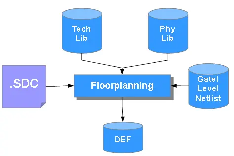
Design Exchange Format – DEF stands for Design Exchange Format. DEF file is a standardized data file that represents the physical layout of design. This file is given as an input to the EDA tool. We can generate this file at every stage of design flow. To send placement information from one stage to another stage. By using this file, we can load the design from one EDA tool to another EDA tool (like from cadence Innovus tool to synopsis ICC tool or vice-versa). Note: LEF files have to load mandatorily before loading the DEF file otherwise an error will rise.
Contents of a Design Exchange Format DEF File
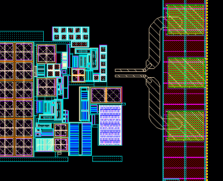
DEF file is used to represent the Physical layout of an Integrated Circuit (IC) in ASCII format. A DEF file is strongly connected with the Library Exchange Format (LEF) file. So both files are needed for a correct display of physical design. DEF file format was developed by Cadence Design System. Whenever we need to transfer the design database from one EDA tool to another EDA tool for further implementation or analysis, we use the DEF file to transfer the design data. For example IR analysis on PnR database or STA on PnR database we transfer the design database in form of a DEF file.
A DEF file contains the design-specific information of the circuit and it is a representation of the design at any point during the physical design. DEF conveys logical design data and physical design data.
Logical design data includes internal connectivity (represented by netlist), group information and physical constraints. Physical data includes placement location and orientation of components and routing geometry.
- Die Area
- Tracks Components (macros)
- I/O Pins
- Nets
- Blockages
- Halo
- Scan Chain
- Vias
- Slots
- Fills
- Region
- Row
- Metal layers
A standard DEF file contains mainly following sections and order of statement is also important.
[ VERSION statement ]

[ DIVIDERCHAR statement ]

[ BUSBITCHARS statement ]

[ DESIGN statement ]

[ TECHNOLOGY statement ]

[ UNITS statements ]

[ DIAAREA statement ]


[ ROW statement ]

[ TRACKS statement ]

[ CELLGRID statement ]

[ VIAS statements ]


[ NONDEFAULTRULES statement ]

[ COMPONENTS statement ]

[ PINS section ]

[ BLOCKAGE section ]


[ FILLS section ]

[ SPECIALNETS section ]

[ NETS section ]

[ SCANCHAINS section ]

[ GROUPS section ]

[ BEGINEXT section ]

END DESIGN statement
Video – Design Exchange Format DEF File of Physical Design Input
https://www.youtube.com/watch?v=pnFJ-ADkxX8
Video – Full Course on Digital VLSI Physical Design
Video – Full Course on Analog or Custom IC Layout Design for Bang Gap Reference
Visit Silicon Synergy to know More
Explore our IC Design Courses in Analog IC Design, Digital Design & Verification


